Datasheet4U Logo Datasheet4U.com

TC551001BFTL-85 - SILICON GATE CMOS STATIC RAM

Download the TC551001BFTL-85 datasheet PDF. This datasheet also covers the TC551001BPL-70 variant, as both devices belong to the same silicon gate cmos static ram family and are provided as variant models within a single manufacturer datasheet.
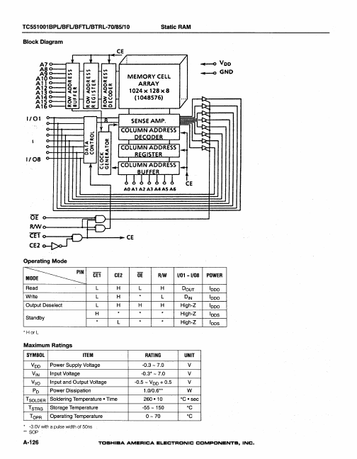
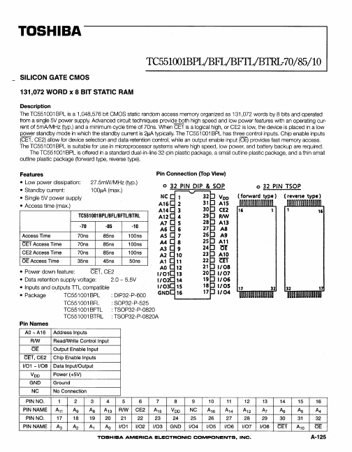
Description

The TC551 001 BPL is a 1,048,576 bit CMOS static random access memory organized as 131,072 words by 8 bits and operated from a single 5V power supply.

Features

  • with an operating current of 5mNMHz (typ. ) and a minimum cycle time of 70ns. When CE1 is a logical high, or CE2 is low, the device is placed in a low power standby mode in which the standby current is 2jJA typically. The TC551 001 BPL has three control inputs. Chip enable inputs (CE1, CE2) allow for device selection and data retention control, while an output enable input (OE) provides fast memory access. The TC551 001 BPL is suitable for use in microprocessor systems where high speed, low power.

📥 Download Datasheet

Note: The manufacturer provides a single datasheet file (TC551001BPL-70-Toshiba.pdf) that lists specifications for multiple related part numbers.

Full PDF Text Transcription (Reference)

The following content is an automatically extracted verbatim text from the original manufacturer datasheet and is provided for reference purposes only.

View original datasheet text
TOSHIBA TC551001BPL/BFL/BFTL/BTRL-70/85/10 SILICON GATE CMOS 131,072 WORD x 8 BIT STATIC RAM Description The TC551 001 BPL is a 1,048,576 bit CMOS static random access memory organized as 131,072 words by 8 bits and operated from a single 5V power supply. Advanced circuit techniques provide both high speed and low power features with an operating current of 5mNMHz (typ.) and a minimum cycle time of 70ns. When CE1 is a logical high, or CE2 is low, the device is placed in a low power standby mode in which the standby current is 2jJA typically. The TC551 001 BPL has three control inputs. Chip enable inputs (CE1, CE2) allow for device selection and data retention control, while an output enable input (OE) provides fast memory access.
Published: |