TC4011BP
TC4011BP/BF/BFT
TOSHIBA CMOS Digital Integrated Circuit Silicon Monolithic
TC4011BP, TC4011BF, TC4011BFT
TC4011B Quad 2 Input NAND Gate
The TC4011B is 2-input positive logic NAND gate respectively. Since all the outputs of these gates are provided with the inverters as buffers, the input/output characteristics have been improved and the variation of propagation delay time due to the increase in load capacity is kept down to the minimum.
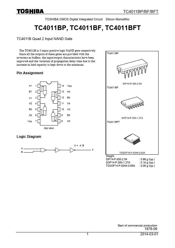
Pin Assignment
A1 1 B1 2 X1 3 X2 4 B2 5 A2 6 VSS 7
(top view)
Logic Diagram
14 VDD 13 A4 12 B4 11 X4 10 X3 9 B3 8 A3
X = A・B
TC4011BF
TC4011BFT
Weight DIP14-P-300-2.54 SOP14-P-300-1.27A TSSOP14-P-0044-0.65A
: 0.96 g (typ.) : 0.18 g (typ.) : 0.06 g (typ.)
Start of mercial production
1978-06 1 2014-03-01
Absolute Maximum Ratings (Note)
TC4011BP/BF/BFT
Characteristics
Symbol
Rating
Unit
DC supply voltage Input voltage Output voltage DC input current Power dissipation Operating temperature range Storage temperature...