TB7109F
Description
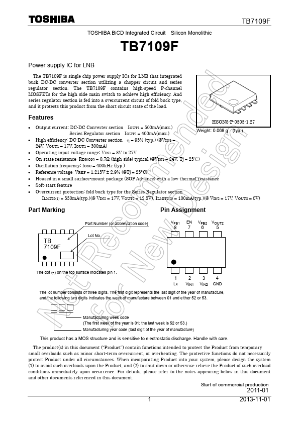
Switch pin This pin is connected to high-side P-channel MOSFET. Input pin This pin is placed in the standby state if VEN=”L”.
Key Features
- High efficiency: DC-DC Converter section η = 95% (typ.) (@VIN1 = 24V, VOUT1 = 17V, IOUT1 = 300mA)
- Operating input voltage range: VIN1 = 8V to 27V
- On-state resistance: RDS(ON) = 0.7Ω (high-side) typical (@VIN1 = 24V, Tj = 25℃)
- Oscillation frequency: fOSC = 400kHz (typ.)
- Reference voltage: VREF = 1.215V ± 2.9% (@Tj = 25°C)
- Housed in a small surface-mount package (SOP Advance) with a low - Soft-start feature
- ) on the top surface indicates pin