TB62705CP
Overview
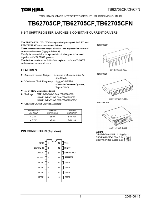
TB62705CP/CF/CFN TOSHIBA Bi−CMOS INTEGRATED CIRCUIT SILICON MONOLITHIC TB62705CP,TB62705CF,TB62705CFN 8-BIT SHIFT REGISTER, LATCHES & CONSTANT-CURRENT DRIVERS The TB62705CP / CF / CFN are specificall...
| Part | TB62705CP |
|---|---|
| Description | 8BIT SHIFT REGISTER / LATCHES & CONSTANT CURRENT DRIVERS |
| Manufacturer | Toshiba |
| Size | 609.06 KB |
TB62705CP/CF/CFN TOSHIBA Bi−CMOS INTEGRATED CIRCUIT SILICON MONOLITHIC TB62705CP,TB62705CF,TB62705CFN 8-BIT SHIFT REGISTER, LATCHES & CONSTANT-CURRENT DRIVERS The TB62705CP / CF / CFN are specificall...
| Part Number | Manufacturer | Description |
|---|---|---|
| TB62709NG | Toshiba | 7-SEGMENT DRIVERS |