The following content is an automatically extracted verbatim text
from the original manufacturer datasheet and is provided for reference purposes only.
View original datasheet text
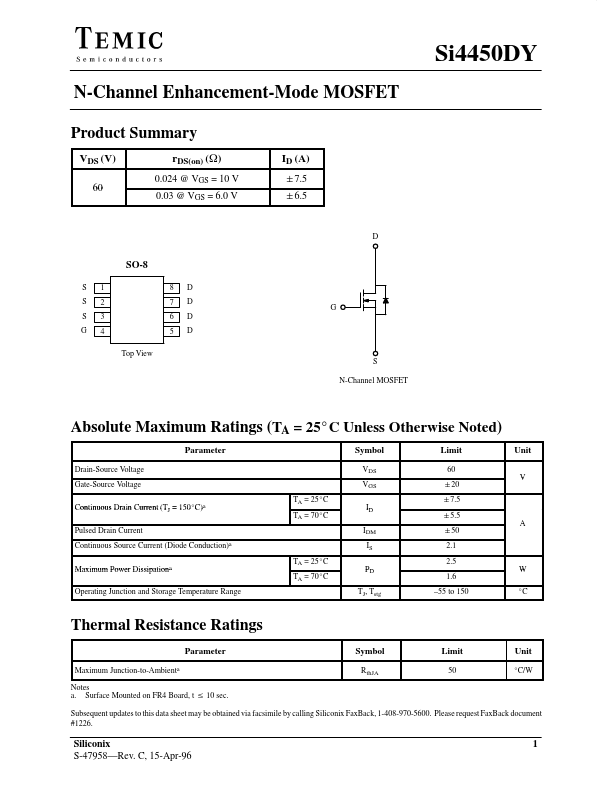
Si4450DY
N-Channel Enhancement-Mode MOSFET
Product Summary
VDS (V)
60
rDS(on) (W)
0.024 @ VGS = 10 V 0.03 @ VGS = 6.0 V
ID (A)
"7.5 "6.5
D
SO-8
S S S G 1 2 3 4 Top View S N-Channel MOSFET 8 7 6 5 D D D D G
Absolute Maximum Ratings (TA = 25_C Unless Otherwise Noted)
Parameter
Drain-Source Voltage Gate-Source Voltage Continuous Drain Current (TJ = 150_C)a Pulsed Drain Current Continuous Source Current (Diode Conduction)a Maximum Power Dissipationa Operating Junction and Storage Temperature Range TA = 25_C TA = 70_C TA = 25_C TA = 70_C
Symbol
VDS VGS ID IDM IS PD TJ, Tstg
Limit
60 "20 "7.5 "5.5 "50 2.1 2.5 1.6 –55 to 150
Unit
V
A
W _C
Thermal Resistance Ratings
Parameter
Maximum Junction-to-Ambienta Notes a. Surface Mounted on FR4 Board, t v 10 sec.
 Si4450DY Datasheet