D High power gain D SMD-package
1
BFS17/BFS17R
1
23
94 9280
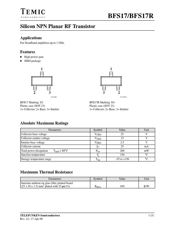
BFS17 Marking: E1 Plastic case (SOT 23) 1= Collector; 2= Base; 3= Emitter
Absolute Maximum Ratings
Parameters
Collector-base voltage
Collector-emitter voltage
Emitter-base voltage
Collector current
Total power dissipation Junction temperature
Tamb ≤ 60°C
Storage temperature range
Maximum Thermal Resistance
Parameters Junction ambient on glass fibre printed board (25 x 20 x 1.5) mm3 plated with 35 mm Cu
32
95 10527
BFS17R Ma.
The following content is an automatically extracted verbatim text
from the original manufacturer datasheet and is provided for reference purposes only.
View original datasheet text
Silicon NPN Planar RF Transistor
Applications
For broadband amplifiers up to 1 GHz.
Features
D High power gain D SMD-package
1
BFS17/BFS17R
1
23
94 9280
BFS17 Marking: E1 Plastic case (SOT 23) 1= Collector; 2= Base; 3= Emitter
Absolute Maximum Ratings
Parameters
Collector-base voltage
Collector-emitter voltage
Emitter-base voltage
Collector current
Total power dissipation Junction temperature
Tamb ≤ 60°C
Storage temperature range
Maximum Thermal Resistance
Parameters Junction ambient on glass fibre printed board (25 x 20 x 1.5) mm3 plated with 35 mm Cu
32
95 10527
BFS17R Marking: E4 Plastic case (SOT 23) 1= Collector; 2= Base; 3= Emitter
Symbol
VCBO VCEO VEBO
IC Ptot Tj Tstg
Value 25 15 2.
 BFS17 Datasheet