CL525 Overview
Key Specifications
Package: TO-92-3
Mount Type: Surface Mount, Through Hole
Pins: 3
Max Voltage (typical range): 90 V
Description
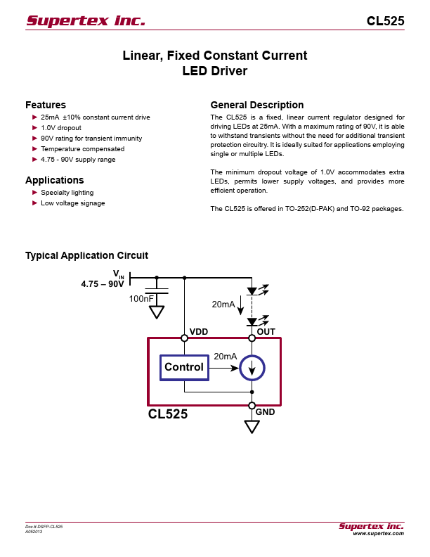
The CL525 is a fixed, linear current regulator designed for driving LEDs at 25mA. With a maximum rating of 90V, it is able to withstand transients without the need for additional transient protection circuitry.
Key Features
- 25mA ±10% constant current drive
- 1.0V dropout
- 90V rating for transient immunity
- Temperature compensated
- 4.75 - 90V supply range