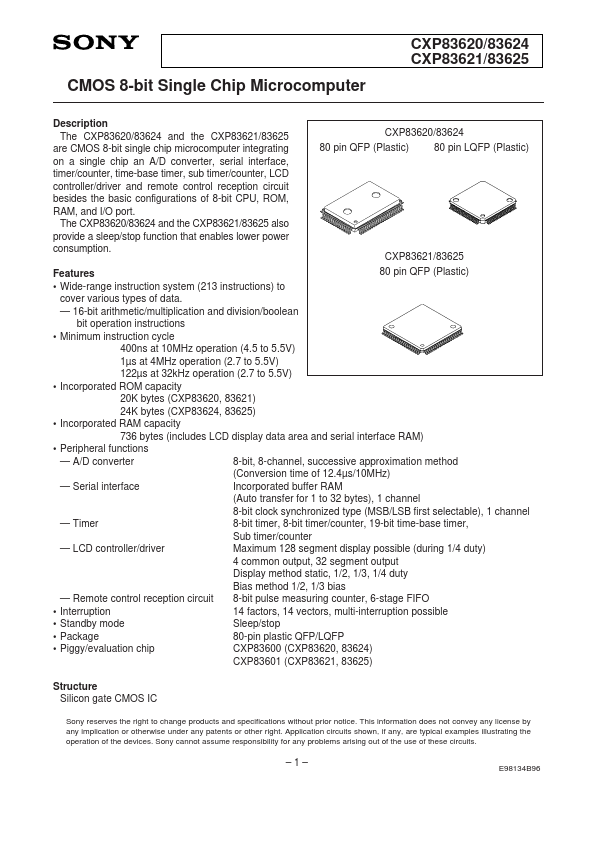
CXP83624
Key Features
- Wide-range instruction system (213 instructions) to cover various types of data. - 16-bit arithmetic/multiplication and division/boolean bit operation instructions
- Minimum instruction cycle 400ns at 10MHz operation (4.5 to 5.5V) 1µs at 4MHz operation (2.7 to 5.5V) 122µs at 32kHz operation (2.7 to 5.5V)
- Incorporated ROM capacity 20K bytes (CXP83620, 83621) 24K bytes (CXP83624, 83625)
- Incorporated RAM capacity 736 bytes (includes LCD display data area and serial interface RAM)
- Peripheral functions - A/D converter 8-bit, 8-channel, successive approximation method (Conversion time of 12.4µs/10MHz) - Serial interface Incorporated buffer RAM (Auto transfer for 1 to 32 bytes), 1 channel 8-bit clock synchronized type (MSB/LSB first selectable), 1 channel - Timer 8-bit timer, 8-bit timer/counter, 19-bit time-base timer, Sub timer/counter - LCD controller/driver Maximum 128 segment display possible (during 1/4 duty) 4 common output, 32 segment output Display method static, 1/2, 1/3, 1/4 duty Bias method 1/2, 1/3 bias - Remote control reception circuit 8-bit pulse measuring counter, 6-stage FIFO
- Interruption 14 factors, 14 vectors, multi-interruption possible
- Standby mode Sleep/stop
- Package 80-pin plastic QFP/LQFP
- Piggy/evaluation chip CXP83600 (CXP83620, 83624) CXP83601 (CXP83621, 83625) Structure Silicon gate CMOS IC Sony reserves the right to