• Part: CXG1045N
  • Description: High Power DPDT Switch
  • Manufacturer: Sony Semiconductor Solutions
  • Size: 64.05 KB
Download CXG1045N Datasheet PDF
Sony Semiconductor Solutions
CXG1045N
CXG1045N is High Power DPDT Switch manufactured by Sony Semiconductor Solutions.
Description The CXG1045N is a DPDT (Dual Pole Dual Throw) antenna switch MMIC used in personal munication handsets such as GSM, GSM1800 or dualband. This IC is designed using the Sony's Ga As J-FET process. Features - 
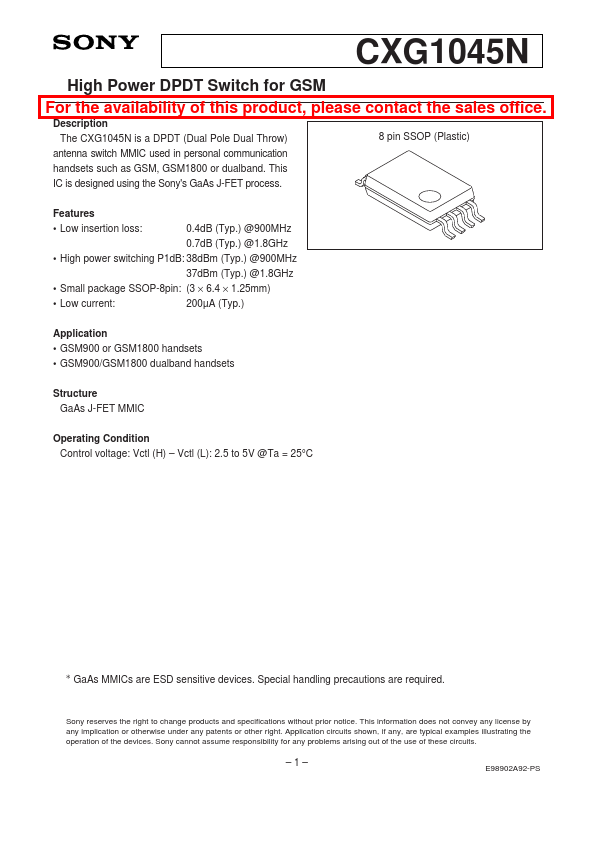
Low insertion loss: 8 pin SSOP (Plastic) 0.4d B (Typ.) @900MHz 0.7d B (Typ.) @1.8GHz - High power switching P1d B: 38d Bm (Typ.) @900MHz 37d Bm (Typ.) @1.8GHz - Small package SSOP-8pin: (3 × 6.4 × 1.25mm) - Low current: 200µA (Typ.) Application - GSM900 or GSM1800 handsets - GSM900/GSM1800 dualband handsets Structure Ga As J-FET MMIC Operating Condition Control voltage: Vctl (H) - Vctl (L): 2.5 to 5V @Ta = 25°C ∗ Ga As MMICs are ESD sensitive devices. Special handling precautions are required. Sony reserves the right to change products and specifications without prior notice. This information does not convey any license by any implication or otherwise under any patents or other right. Application circuits shown, if any, are typical examples illustrating the operation of the devices. Sony cannot assume responsibility for any problems arising out of the use of these circuits. - 1- E98902A92-PS Block Diagram RF1 RF4 RF2 RF3 VCTLA High Low VCTLB Low High RF1 - RF2, RF3 - RF4 ON RF2 - RF3, RF4 - RF1 OFF RF1 - RF2, RF3 - RF4 OFF RF2 - RF3, RF4 - RF1 ON Electrical Characteristics (1) Item Insertion loss Symbol ∗3, ∗4 IL ∗1, ∗2, ∗5 ∗3, ∗4 Isolation VSWR 2nd harmonics ISO VSWR 2fo ∗1, ∗2, ∗5 ∗1 to ∗5 ∗1, ∗2 ∗3 ∗1, ∗2 3rd harmonics 3fo ∗3 ∗3 Input power for 1d B pression Switching time Control current ∗1 ∗2 ∗3 ∗4 ∗5 P1d B TSW I CTL 0/5V control ∗1, ∗2 36 35 38 37 100 200 18 15 Condition Min. Typ. 0.4 0.7 21 17 1.2 1.4 (Ta = 25°C) Max. 0.7 1.0 Unit d B d B d B d B - 31 - 31 - 31 - 31 d Bm d Bm d Bm d Bm d Bm d Bm 500 350 ns µA RF Input terminal is RF2. (RF2 → RF1, RF2 → RF3), Pin = 32d Bm, 1710 to 1785MHz, 0/5V control RF Input terminal is RF4. (RF4 → RF1, RF4 → RF3), Pin = 32d Bm, 1710 to 1785MHz, 0/5V control RF Input terminal is RF4. (RF4 → RF1, RF4 → RF3),...