CXA1787N Overview
Description
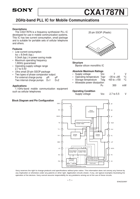
The CXA1787N is a frequency synthesizer PLL IC developed for use in mobile communication systems. This IC has low current consumption, small package and is suitable for portable sets of cellular telephone and others.
Key Features
- Low current consumption Icc = 8.0mA (typ.) 0.3mA (typ.) in power saving mode
- Maximum operating frequency 1.8GHz guaranteed
- Operating supply voltage range 2.7 to 5.5V
- Ultra small 20-pin SSOP package
- Operating temperature Topr