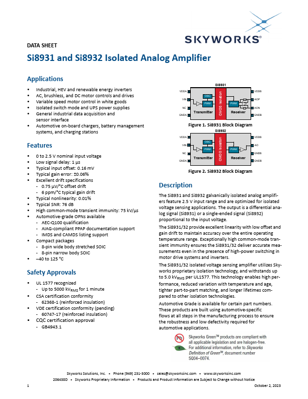
Datasheet4U Logo Datasheet4U.com

Si8932 - Isolated Analog Amplifier

Download the Si8932 datasheet PDF. This datasheet also covers the Si8931 variant, as both devices belong to the same isolated analog amplifier family and are provided as variant models within a single manufacturer datasheet.

General Description

The Si8931 and Si8932 galvanically isolated analog amplifiers feature 2.5 V input range and are optimized for isolated voltage sensing applications.

The output is a differential analog signal (Si8931) or a single-ended signal (Si8932) proportional to the input voltage.

Key Features

  • 0 to 2.5 V nominal input voltage.
  • Low signal delay: 1 µs.
  • Typical input offset: 0.16 mV.
  • Typical gain error: ±0.06%.
  • Excellent drift specifications - 0.75 µV/°C offset drift - 6 ppm/°C typical gain drift.
  • Typical nonlinearity: 0.01%.
  • Typical SNR: 76 dB.
  • High common-mode transient immunity: 75 kV/µs.
  • Automotive-grade OPNs available - AEC-Q100 qualification - AIAG-compliant PPAP documentation support - IMDS and CAMDS.

📥 Download Datasheet

Note: The manufacturer provides a single datasheet file (Si8931-SkyworksSolutions.pdf) that lists specifications for multiple related part numbers.

Datasheet Details

Part number Si8932
Manufacturer Skyworks Solutions
File Size 1.63 MB
Description Isolated Analog Amplifier
Datasheet download datasheet Si8932 Datasheet

Full PDF Text Transcription (Reference)

The following content is an automatically extracted verbatim text from the original manufacturer datasheet and is provided for reference purposes only.

View original datasheet text
DATA SHEET Si8931 and Si8932 Isolated Analog Amplifier Applications • Industrial, HEV and renewable energy inverters • AC, brushless, and DC motor controls and drives • Variable speed motor control in white goods • Isolated switch mode and UPS power supplies • General industrial data acquisition and sensor interface • Automotive on-board chargers, battery management systems, and charging stations Features • 0 to 2.5 V nominal input voltage • Low signal delay: 1 µs • Typical input offset: 0.16 mV • Typical gain error: ±0.06% • Excellent drift specifications - 0.75 µV/°C offset drift - 6 ppm/°C typical gain drift • Typical nonlinearity: 0.