CLA4610-085LF Key Features
- Low thermal resistance: 73 °C/W
- Typical threshold level: +16 dBm @ 2.6 GHz
- Low capacitance: 0.32 pF
- Low-profile, ultra-miniature QFN (3-pin, 2 x 2 mm) package (MSL1, 260 C per JEDEC J-STD-020)
CLA4610-085LF is Surface Mount Limiter Diode manufactured by Skyworks Solutions.
| Part Number | Description |
|---|---|
| CLA4610-000 | Silicon Limiter Diode Bondable Chips |
| CLA4611-000 | Silicon Limiter Diode Bondable Chips |
| CLA4611-085LF | Surface Mount Limiter Diode |
| CLA4601-000 | Silicon Limiter Diode Bondable Chips |
| CLA4602-000 | Silicon Limiter Diode Bondable Chips |
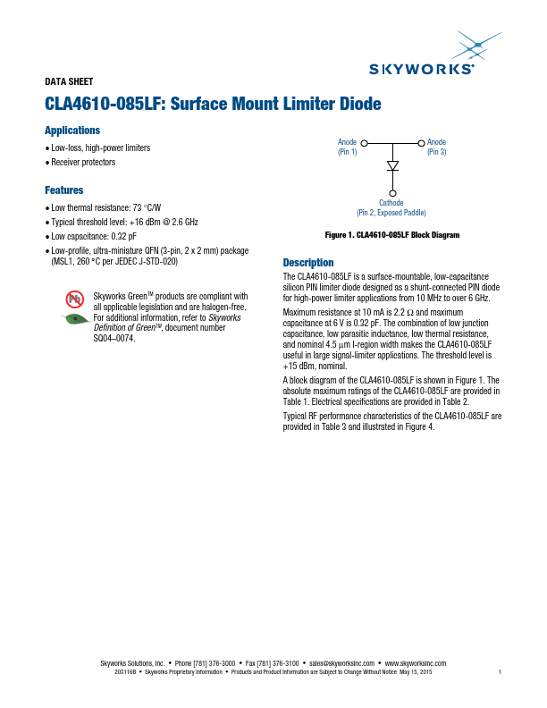
The CLA4610-085LF is a surface-mountable, low-capacitance silicon PIN limiter diode designed as a shunt-connected PIN diode for high-power limiter applications from 10 MHz to over 6 GHz. Maximum resistance at 10 mA is 2.2 Ω and maximum capacitance at 6 V is 0.32 pF. The bination of low junction capacitance, low parasitic inductance, low , and nominal 4.5 μm I-region width makes the CLA4610-085LF useful in large...