• Part: SSF9926
  • Description: PWM applications
  • Manufacturer: Silikron Semiconductor Co
  • Size: 422.31 KB
Download SSF9926 Datasheet PDF
Silikron Semiconductor Co
SSF9926
SSF9926 is PWM applications manufactured by Silikron Semiconductor Co.
DESCRIPTION 
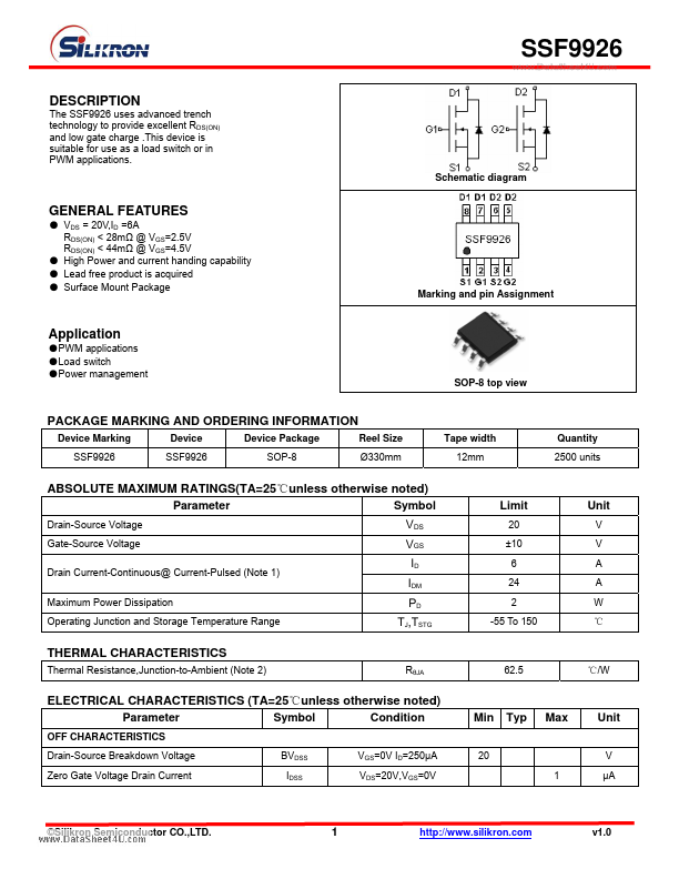
The SSF9926 uses advanced trench technology to provide excellent RDS(ON) and low gate charge .This device is suitable for use as a load switch or in PWM applications. Schematic diagram GENERAL FEATURES - VDS = 20V,ID =6A RDS(ON) < 28mΩ @ VGS=2.5V RDS(ON) < 44mΩ @ VGS=4.5V - High Power and current handing capability - Lead free product is acquired - Surface Mount Package Marking and pin Assignment Application - PWM applications - Load switch - Power management SOP-8 top view PACKAGE MARKING AND ORDERING INFORMATION Device Marking SSF9926 Device SSF9926 Device Package SOP-8 Reel Size Ø330mm Tape width 12mm Quantity 2500 units ABSOLUTE MAXIMUM RATINGS(TA=25℃unless otherwise noted) Parameter Symbol Drain-Source Voltage Gate-Source Voltage Drain Current-Continuous@ Current-Pulsed (Note 1) Maximum Power Dissipation Operating Junction and Storage Temperature Range Limit 20 ±10 6 24 2 -55 To 150 Unit V V A A W ℃ VDS VGS ID IDM PD TJ,TSTG THERMAL CHARACTERISTICS Thermal Resistance,Junction-to-Ambient (Note 2) RθJA 62.5 ℃/W ELECTRICAL CHARACTERISTICS (TA=25℃unless otherwise noted) Parameter Symbol Condition OFF CHARACTERISTICS Drain-Source Breakdown Voltage Zero Gate Voltage Drain Current BVDSS IDSS VGS=0V ID=250μA VDS=20V,VGS=0V Min Typ Max Unit μA ©Silikron Semiconductor CO.,LTD. 1 http://.silikron. v1.0 .. Gate-Body Leakage Current ON CHARACTERISTICS (Note 3) Gate Threshold Voltage Drain-Source On-State Resistance Forward Transconductance DYNAMIC CHARACTERISTICS (Note4) Input Capacitance Output Capacitance Reverse Transfer Capacitance SWITCHING CHARACTERISTICS (Note 4) Turn-on Delay Time Turn-on Rise Time Turn-Off Delay Time Turn-Off Fall Time Total Gate Charge Gate-Source Charge Gate-Drain Charge DRAIN-SOURCE DIODE CHARACTERISTICS Diode Forward Voltage (Note 3) IGSS VGS=±10V,VDS=0V ±100 n...