SSF3428
DESCRIPTION
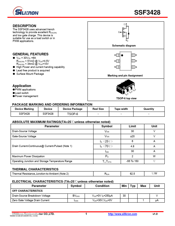
The SSF3428 uses advanced trench technology to provide excellent RDS(ON) and low gate charge .This device is suitable for use as a load switch or in PWM applications. Schematic diagram
GENERAL FEATURES
- VDS = 30V,ID =6A RDS(ON) < 51mΩ @ VGS=4.5V RDS(ON) < 34mΩ @ VGS=10V
- High Power and current handing capability
- Lead free product is acquired
- Surface Mount Package
Marking and pin Assignment
Application
- PWM applications
- Load switch
- Power management
TSOP-6 top view
PACKAGE MARKING AND ORDERING INFORMATION
Device Marking SSF3428 Device SSF3428 Device Package Reel Size Tape width Quantity
- TSOP-6
ABSOLUTE MAXIMUM RATINGS(TA=25℃unless otherwise noted) Parameter Symbol
Drain-Source Voltage Gate-Source Voltage
Limit
30 ±20 6 4.8 30 2 -55 To 150
Unit
V V A A A W ℃
VDS VGS ID(25℃) ID(70℃) IDM PD TJ,TSTG
Drain Current-Continuous@ Current-Pulsed (Note 1)
Maximum Power Dissipation Operating Junction and Storage Temperature Range
THERMAL CHARACTERISTICS
Thermal...