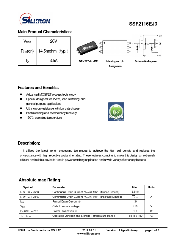
SSF2116EJ3 Overview
Description
It utilizes the latest trench processing techniques to achieve the high cell density and reduces the on-resistance with high repetitive avalanche rating. These features combine to make this design an extremely efficient and reliable device for use in power switching application and a wide variety of other applications Absolute max Rating: Symbol ID @ TC = 25°C ID @ TC = 25°C IDM VGS PD @TC = 25°C TJ TSTG Parameter Continuous Drain Current, VGS @ 10V (Silicon Limited) Continuous Drain Current, VGS @ 10V (Package Limited) Pulsed Drain Current ② Gate to sou.
Key Features
- Advanced MOSFET process technology
- Special designed for PWM, load switching and general purpose applications
- Ultra low on-resistance with low gate charge
- Fast switching and reverse body recovery
- 150℃ operating temperature