The following content is an automatically extracted verbatim text
from the original manufacturer datasheet and is provided for reference purposes only.
View original datasheet text
n-chalrlnel JFETs
design4!d for • • •
• Small-Si~lnal Amplifiers • Switche:s
H
Performance Curves NP See Section 4
BENEFITS • Operates from High Supply
Voltages BVGSS> 50V
*ABSOLUTE MAXIMUM RATINGS (25°C)
Gate-Drain or Gate·Source Voltage (Note 1) .... , ... -50 V Gate Current .... , ........ , .. , , ...... ' ...... 10 mA Total Device Dissipation at (or below) 25°C
Free-Air Temperature (Note 2) .............. 300mW
Storage Temperature Range .... , ......... -65 to +200°C
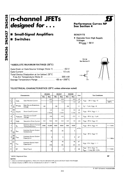
TO-1S See Section 5
"~:
-r~
I
G.
 2N3436 Datasheet