2N2844 Overview
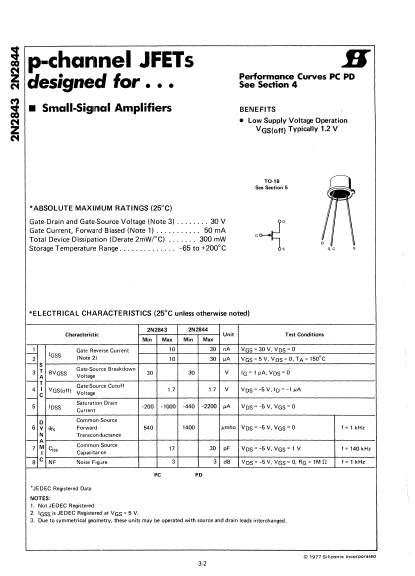
p-cha.,.nel JFETs designed for Small-Siglllal Amplifiers H Performance Curves PC PD See Section 4 BENEFITS Low Supply Voltage Operation V GS(off) Typically 1.2 V RATINGS (25°C) Gate-Drain and Gate-Source Voltage (Note 3) ........ 30V Gate Current, Forwal"d Biased (Note 1) ........... 50mA Total Device Dissipation (Derate 2mW/oC) .......