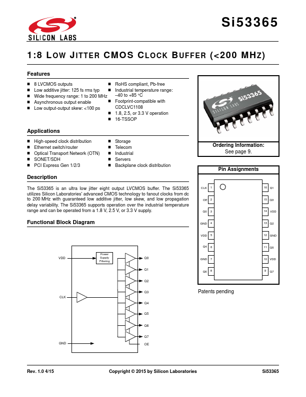
Datasheet4U Logo Datasheet4U.com

SI53365 - 1:8 LOW JITTER CMOS CLOCK BUFFER

Description

The Si53365 is an ultra low jitter eight output LVCMOS buffer.

The Si53365 utilizes Silicon Laboratories' advanced CMOS technology to fanout clocks from dc to 200 MHz with guaranteed low additive jitter, low skew, and low propagation delay variability.

Features

  • 8 LVCMOS outputs.
  • RoHS compliant, Pb-free.
  • Low additive jitter: 125 fs rms typ.
  • Industrial temperature range:.
  • Wide frequency range: 1 to 200 MHz.
  • 40 to +85 °C.
  • Asynchronous output enable.
  • Footprint-compatible with.
  • Low output-output skew:.

📥 Download Datasheet

Other Datasheets by Silicon Laboratories

Full PDF Text Transcription

Click to expand full text
Si53365 1:8 LOW JITTER CMOS CLOCK BUFFER (<200 MHZ) Features  8 LVCMOS outputs  RoHS compliant, Pb-free  Low additive jitter: 125 fs rms typ  Industrial temperature range:  Wide frequency range: 1 to 200 MHz –40 to +85 °C  Asynchronous output enable  Footprint-compatible with  Low output-output skew: <100 ps CDCLVC1108  1.8, 2.5, or 3.3 V operation  16-TSSOP Applications  High-speed clock distribution  Ethernet switch/router  Optical Transport Network (OTN)  SONET/SDH  PCI Express Gen 1/2/3  Storage  Telecom  Industrial  Servers  Backplane clock distribution Description The Si53365 is an ultra low jitter eight output LVCMOS buffer.
Published: |