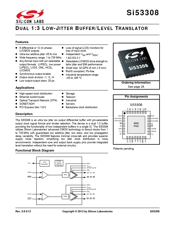
SI53308 Description
The Si53308 is an ultra low jitter six output differential buffer with pin-selectable output clock signal format and divider selection. The device is a dual 1:3 buffer providing the functionality of two independent buffers in a single IC. The Si53308 utilizes Silicon Laboratories' advanced CMOS technology to fanout clocks from 1 to 725 MHz with guaranteed low additive jitter, low skew, and low propagation delay...
SI53308 Key Features
- 6 differential or 12 (in phase)
- Ultra-low additive jitter: 45 fs rms
- Independent VDD and VDDO
- Wide frequency range: 1 to 725 MHz 1.8/2.5/3.3 V
- Any-format input with pin selectable
- Selectable LVCMOS drive strength to output formats: LVPECL, low power tailor jitter and EMI performance
- Synchronous output enable
- Output clock division: /1, /2, /4
- Low output-output skew: 25 ps
- Small size: 32-QFN (5 mm x 5 mm)