CY2SSTV857-32
CY2SSTV857-32 is Differential Clock Buffer/Driver DDR400/PC3200-Compliant manufactured by Silicon Labs.
Differential Clock Buffer/Driver DDR400/PC3200-pliant
Features
- Operating frequency: 60 MHz to 230 MHz
- Supports 400 MHz DDR SDRAM
- 10 differential outputs from one differential input
- Spread-Spectrum-patible
- Low jitter (cycle-to-cycle): < 75
- Very low skew: < 100 ps
- Power management control input
- High-impedance outputs when input clock < 20 MHz
- 2.6V operation
- Pin-patible with CDC857-2 and -3
- 48-pin TSSOP and 40 QFN package
- Industrial temperature of
- 40°C to 85°C
- Conforms to JEDEC DDR specification
Description
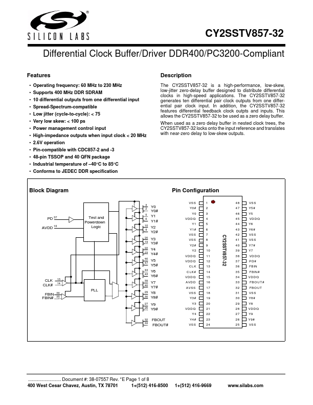
The CY2SSTV857-32 is a high-performance, low-skew, low-jitter zero-delay buffer designed to distribute differential clocks in high-speed...