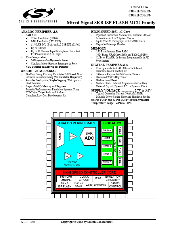
C8051F206
C8051F220/1/6
C8051F230/1/6
TABLE OF CONTENTS
1. SYSTEM OVERVIEW ........................................................................................................6
Table 1.1.1. Product Selection Guide ................................................................................................................6
Figure 1.1. C8051F206, C8051F220 and C8051F226 Block Diagram (48 TQFP) ..........................................7
Figure 1.2 C8051F221 Block Diagram (32 LQFP) ...........................................................................................8
Figure 1.3 C8051F230 and C8051F236 Block Diagram (48 TQFP) ................................................................9
Figure 1.4 C8051F231 Block Diagram (32 LQFP) .........................................................................................10
1.1. CIP-51TM Microcontroller Core.............................................................................................................11
Figure 1.5. Comparison of Peak MCU Throughputs.......................................................................................11
Figure 1.6. On-Board Clock and Reset............................................................................................................12
1.2. On-Board Memory.................................................................................................................................13
Figure 1.7. On-Board Memory Map................................................................................................................13
1.3. JTAG .....................................................................................................................................................14
Figure 1.8. Debug Environment Diagram .......................................................................................................14
1.4. Digital/Analog Configurable I/O ...........................................................................................................15
Figure 1.9. Port I/O Functional Block Diagram ..............................................................................................15
1.5. Serial Ports.............................................................................................................................................15
1.6. Analog to Digital Converter ..................................................................................................................16
Figure 1.10. ADC Diagram .............................................................................................................................16
1.7. Comparators...........................................................................................................................................17
Figure 1.11. Comparator Diagram...................................................................................................................17
2. ABSOLUTE MAXIMUM RATINGS*.............................................................................18
3. GLOBAL DC ELECTRICAL CHARACTERISTICS ...................................................19
4. PINOUT AND PACKAGE DEFINITIONS ....................................................................20
Table 4.1 Pin Definitions.................................................................................................................................20
Figure 4.1 TQFP-48 Pin Diagram ....................................................................................................................22
Figure 4.2 LQFP-32 Pin Diagram ....................................................................................................................23
Figure 4.3 TQFP-48 Package Drawing ............................................................................................................24
Figure 4.4 LQFP-32 Package Drawing ...........................................................................................................25
5. ADC (8-Bit, C8051F220/1/6 Only) ....................................................................................26
Figure 5.1. 8-Bit ADC Functional Block Diagram..........................................................................................26
5.1. Analog Multiplexer and PGA................................................................................................................26
5.2. ADC Modes of Operation......................................................................................................................26
Figure 5.2. 12-Bit ADC Track and Conversion Example Timing...................................................................27
Figure 5.3. AMX0SL: AMUX Channel Select Register .................................................................................28
Figure 5.4. ADC0CF: ADC Configuration Register .......................................................................................29
Figure 5.5. ADC0CN: ADC Control Register (C8051F220/1/6 and C8051F206) .........................................30
Figure 5.6. ADC0H: ADC Data Word Register (C8051F220/1/6 and C8051F206)......................................31
5.3. ADC Programmable Window Detector.................................................................................................31
Figure 5.7. ADC0GTH: ADC Greater-Than Data Register (C8051F220/1/6 and C8051F206) .....................31
Figure 5.8. ADC0LTH: ADC Less-Than Data Byte Register (C8051F220/1/6 and C8051F206)..................31
Figure 5.9. 8-Bit ADC Window Interrupt Examples.......................................................................................32
Table 5.1. 8-Bit ADC Electrical Characteristics..............................................................................................33
6. ADC (12-Bit, C8051F206 Only) ........................................................................................34
Figure 6.1. 12-Bit ADC Functional Block Diagram........................................................................................34
6.1. Analog Multiplexer and PGA................................................................................................................34
6.2. ADC Modes of Operation......................................................................................................................34
Figure 6.2. 12-Bit ADC Track and Conversion Example Timing...................................................................35
Figure 6.3. AMX0SL: AMUX Channel Select Register .................................................................................36
Figure 6.4. ADC0CF: ADC Configuration Register (C8051F220/1/6 and C8051F206) ................................37
Figure 6.5. ADC0CN: ADC Control Register (C8051F220/1/6 and C8051F206) .........................................38
Figure 6.6. ADC0H: ADC Data Word MSB Register (C8051F206) .............................................................39
Rev. 1.4
2