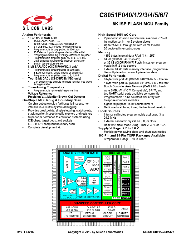
C8051F040
C8051F040 is 8K ISP FLASH MCU manufactured by Silicon Labs.
C8051F040/1/2/3/4/5/6/7
Mixed Signal ISP Flash MCU Family
Analog Peripherals
- 10 or 12-Bit SAR ADC
- -
- -
- -
- -
- - ..
- -
8-bit SAR ADC (C8051F040/1/2/3 only)
12-bit (C8051F040/1) or 10-bit (C8051F042/3/4/5/6/7) resolution ± 1 LSB INL, guaranteed no missing codes Programmable throughput up to 100 ksps 13 External Inputs; single-ended or differential SW programmable high voltage difference amplifier Programmable amplifier gain: 16, 8, 4, 2, 1, 0.5 Data-dependent windowed interrupt generator Built-in temperature sensor Programmable throughput up to 500 ksps 8 External Inputs, single-ended or differential Programmable amplifier gain: 4, 2, 1, 0.5 Can synchronize outputs to timers for jitter-free waveform generation Programmable hysteresis/response time
Memory
- 4352 bytes internal data RAM (4 k + 256)
- 64 k B (C8051F040/1/2/3/4/5) or 32 k B (C8051F046/7) Flash; in-system programmable in 512-byte sectors External 64 k B data memory interface (programmable multiplexed or non-multiplexed modes)
Digital Peripherals
- 8 byte-wide port I/O (C8051F040/2/4/6); 5 V tolerant
- 4 byte-wide port I/O (C8051F041/3/5/7); 5 V tolerant
- Bosch Controller Area Network (CAN 2.0B), hardware SMBus™ (I2C™ patible), SPI™, and two UART serial ports available concurrently Programmable 16-bit counter/timer array with 6 capture/pare modules 5 general purpose 16-bit counter/timers Dedicated watch-dog timer; bi-directional reset pin
Two 12-bit DACs (C8051F040/1/2/3 only)
- -
Three Analog parators
- Voltage Reference
- Precision VDD Monitor/Brown-Out Detector On-Chip JTAG Debug & Boundary Scan
- On-chip debug circuitry facilitates full- speed, nonintrusive in-circuit/in-system debugging Provides breakpoints, single-stepping, watchpoints, stack monitor; inspect/modify memory and registers Superior performance to emulation systems using ICE-chips, target pods, and sockets IEEE1149.1 pliant boundary scan plete development kit
Clock Sources
- Internal...