LT251A
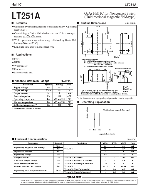
Features s Outline Dimensions 2.7±0.3 ¡Operation by small magnet due to high sensitivity Operating point<30m T Y ¡ bining a Ga As Hall device and an IC in a pact 1 4 package (2.9X1.5X1.1mm) ¡Wide operation temperature range obtained by Ga As Hall device (-20 to +125˚C) ¡Long life time due to noncontact-type
X s Applications ¡FDD ¡HDD ¡Water meter ¡Car stereo ¡Microswitch, etc.
0.16+0.10 -0.06
1.1-0.1
+0.2
4-R0.2 Hall device center line X : +0.05±0.23mm against package center Y : -0.05±0.1mm against package lead center between No.2 and No.3 terminals Z : 0.81±0.15mm from package surface Terminal connections 1.5±0.2 0.6 0.6 REG Hall + device H
- s Absolute Maximum Ratings
Parameter Supply voltage Output voltage Output current Power dissipation Operating temperature Storage temperature Soldering temperature- 1
- 1 Soldering time : within 10 seconds
(Ta=25˚C) Unit V V m A m W ˚C ˚C ˚C
Symbol Rating VCC 18 VOUT 18 IO 5 PD 100 Topr -20 to +125 -55 to +150 Tstg...