LH28F020SU-N Overview
Key Specifications
Package: SOP
Operating Voltage: 5 V
Max Voltage (typical range): 5.5 V
Min Voltage (typical range): 4.5 V
Key Features
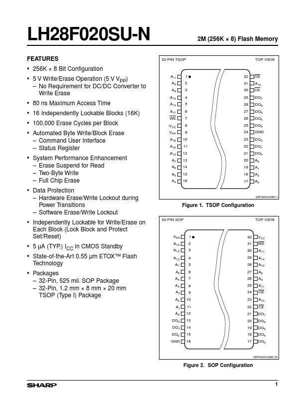
- Flash Memory TOP VIEW
- 256K × 8 Bit Configuration
- System Performance Enhancement
- Data Protection – Hardware Erase/Write Lockout during Power Transitions – Software Erase/Write Lockout 28F020SUN80-1 Figure
- TSOP Configuration 32-PIN SOP TOP VIEW