LH28F020SU-L Overview
Key Features
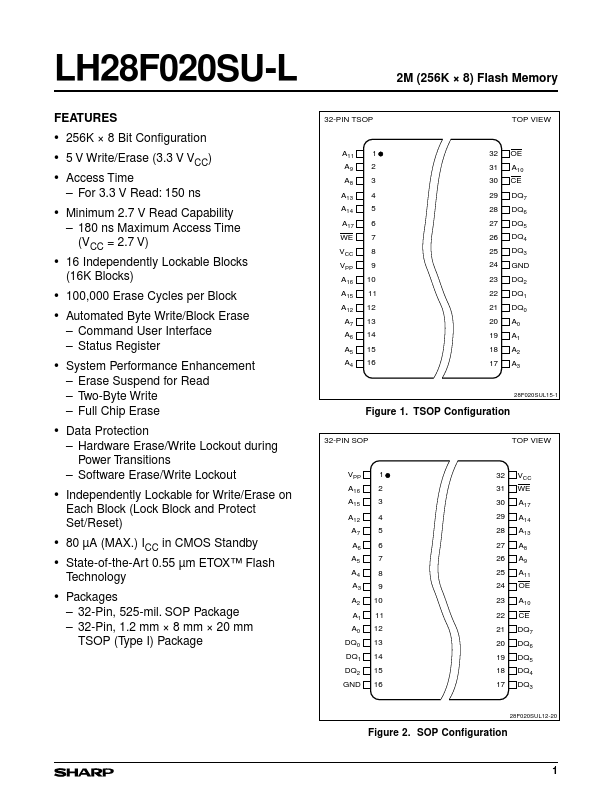
- Flash Memory TOP VIEW
- 256K × 8 Bit Configuration
- 5 V Write/Erase (3.3 V VCC)
- Minimum 2.7 V Read Capability – 180 ns Maximum Access Time (VCC = 2.7 V)
- 16 Independently Lockable Blocks (16K Blocks)
| Part | LH28F020SU-L |
|---|---|
| Description | 2M (256K bb 8) Flash Memory |
| Manufacturer | Sharp Corporation |
| Size | 245.48 KB |
| Part Number | Manufacturer | Description |
|---|---|---|
| W25Q128JV | Winbond | 3V 128M-BIT SERIAL FLASH MEMORY |
| 25Q128JVSM | Winbond | 3V 128M-BIT SERIAL FLASH MEMORY |
| W25Q256JV | Winbond | 3V 256M-BIT SERIAL FLASH MEMORY |