S-8209B Overview
Key Specifications
Package: TSSOP
Operating Voltage: 1.8 V
Max Voltage (typical range): 8 V
Min Voltage (typical range): 1.5 V
Key Features
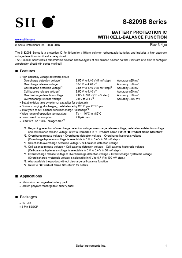
- Overcharge detection voltage *1
- Overcharge release voltage 3.50 V to 4.40 V*2
- Cell-balance detection voltage*1 3.55 V to 4.40 V (5 mV step)*3 *1
- Cell-balance release voltage 3.50 V to 4.40 V*4
- Overdischarge detection voltage 2.0 V to 3.0 V (10 mV step) *5
