Description
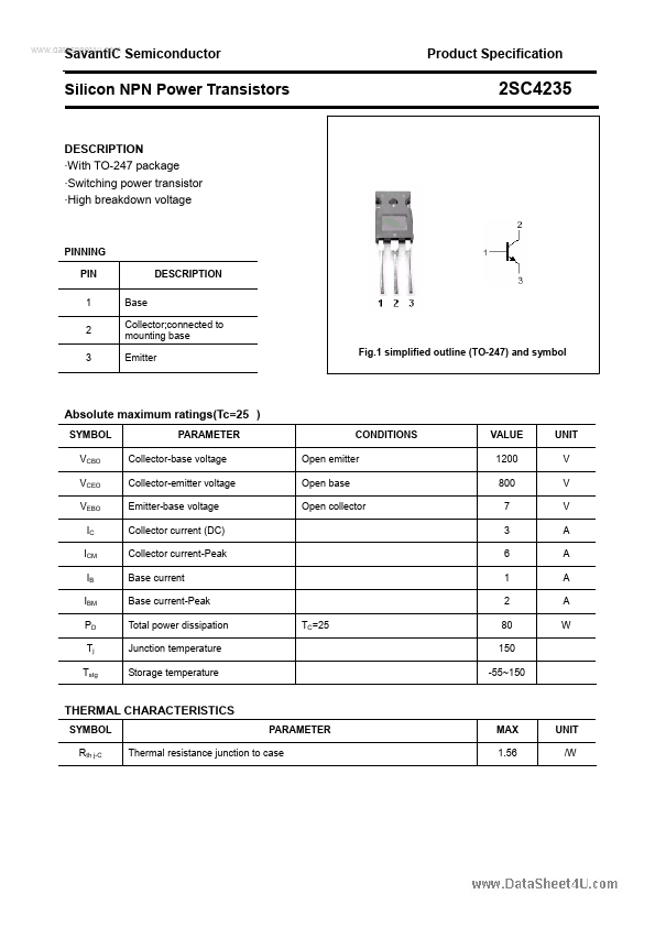
With TO-247 package - Switching power transistor - High breakdown voltage PINNING PIN DESCRIPTION 1 Base 2 Collector;connected to mounting base 3 Emitter Fig.1 simplified outline (TO-247) and symbol SYMBOL PARAMETER VCBO Collector-base voltage VCEO Collector-emitter voltage VEBO IC Emitter-base voltage Collector current (DC) ICM Collector current-Peak IB Base current IBM Base current-Peak PD Total power dissipation Tj Junction temperature Tstg Storage temperature CONDITIONS Open emitter Open base Open collector TC=25 SYMBOL PARAMETER Rth j-C VALUE 1200 800 7 3 6 1 2 80 150 -55~150 UNIT V V V A A A A W MAX 1.56 UNIT /W .datSasaheveat4nu.tcIoCm Semiconductor Silicon NPN Power Transistors Product Specification 2SC4235 CHARACTERISTICS Tj=25 unless otherwise specified SYMBOL PARAMETER CONDITIONS VCEO(SUS) Collector-emitter sustaining voltage IC=0.1A; IB=0 VCEsat Collector-emitter saturation voltage IC=1.5A ;IB=0.3A VBEsat Base-emitter saturation voltage IC=1.5A ;IB=0.3A ICBO Collector cut-off current ICEO Collector cut-off current At rated voltage IEBO Emitter cut-off current At rated voltage hFE-1 DC current gain IC=1.5A ; VCE=5V hFE-2 DC current gain IC=1mA ; VCE=5V fT Transition frequency IC=0.3A ; VCE=10V Switching times resistive load ton Turn-on time ts Storage time tf Fall time IC=1.5A IB1=0.3A; IB2=0.6A VBB2=4V ,RL=170C MIN TYP. MAX UNIT 800 V 1.0 V 1.5 V 0.1 mA 0.1 mA 8 7 8 MHz 0.5 µs 3.5 µs 0.3 µs 2 .datSasaheveat4nu.tcIoCm Semiconductor Silicon NPN Power Transistors PACKAGE OUTLINE Product Specification 2SC4235 Fig.2 Outline dimensions 3.