2N6687 Overview
Key Specifications
Description
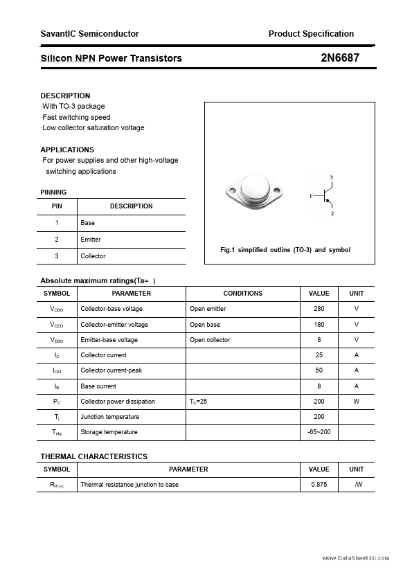
With TO-3 package - Fast switching speed - Low collector saturation voltage APPLICATIONS - For power supplies and other high-voltage switching applications PINNING PIN 1 2 3 Base Emitter Collector Fig.1 simplified outline (TO-3) and symbol DESCRIPTION SYMBOL VCBO VCEO VEBO IC ICM IB PC Tj Tstg PARAMETER Collector-base voltage Collector-emitter voltage Emitter-base voltage Collector current Collector current-peak Base current Collector power dissipation Junction temperature Storage temperature TC=25 CONDITIONS Open emitter Open base Open collector VALUE 280 180 8 25 50 8 200 200 -65~200 UNIT V V V A A A W SYMBOL Rth j-c PARAMETER SavantIC Semiconductor Product Specification Silicon NPN Power Transistors CHARACTERISTICS Tj=25 unless otherwise specified PARAMETER CONDITIONS MIN TYP. 2N6687 SYMBOL MAX UNIT VCEO(SUS) Collector-emitter sustaining voltage IC=0.2A ;IB=0 180 V VCEsat Collector-emitter saturation voltage IC=25A; IB=2.5A 1.5 V VBEsat Base-emitter saturation voltage IC=25A; IB=2.5A 1.8 V ICEV Collector cut-off current VCE=280V; VBE=-1.5V 50 µA IEBO Emitter cut-off current VEB=8V; IC=0 100 µA hFE-1 DC current gain IC=1A ; VCE=2V 30 hFE-2 DC current gain IC=10A ; VCE=2V 25 100 hFE-3 DC current gain IC=25A ; VCE=2V 15 fT Transition frequency IC=1A ; VCE=10V 20 100 MHz 2 SavantIC Semiconductor Product Specification Silicon NPN Power Transistors PACKAGE OUTLINE 2N6687 Fig.2 outline dimensions (unindicated tolerance:±0.1mm) 3.