2N4910 Overview
Description
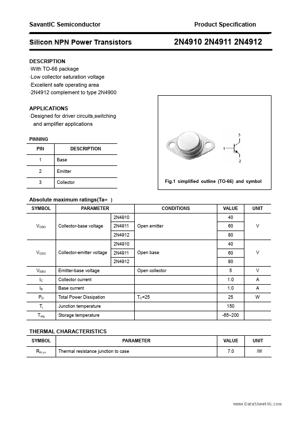
With TO-66 package - Low collector saturation voltage - Excellent safe operating area - 2N4912 complement to type 2N4900 APPLICATIONS - Designed for driver circuits,switching and amplifier applications PINNING PIN 1 2 3 Base Emitter Collector DESCRIPTION 2N4910 2N4911 2N4912 Fig.1 simplified outline (TO-66) and symbol SYMBOL PARAMETER 2N4910 VCBO Collector-base voltage 2N4911 2N4912 2N4910 VCEO Collector-emitter voltage 2N4911 2N4912 VEBO IC IB PD Tj Tstg Emitter-base voltage Collector current Base current Total Power Dissipation Junction temperature Storage temperature TC=25 Open collector Open base Open emitter CONDITIONS VALUE 40 60 80 40 60 80 5 1.0 1.0 25 150 -65~200 V A A W V V UNIT SYMBOL Rth j-c PARAMETER SavantIC Semiconductor Product Specification Silicon NPN Power Transistors CHARACTERISTICS Tj=25 unless otherwise specified PARAMETER 2N4910 VCEO(SUS) Collector-emitter sustaining voltage 2N4911 2N4912 VCEsat VBEsat VBE Collector-emitter saturation voltage Base-emitter saturation voltage Base-emitter on voltage 2N4910 ICEO Collector cut-off current 2N4911 2N4912 ICEX ICBO IEBO hFE-1 hFE-2 hFE-3 COB fT Collector cut-off current Collector cut-off current Emitter cut-off current DC current gain DC current gain DC current gain Output capacitance Transition frequency IC=1A; IB=0.1A IC=1A ;IB=0.1A IC=1A ; VCE=1V VCE=20V; IB=0 VCE=30V; IB=0 VCE=40V; IB=0 IC=0.1A ;IB=0 SYMBOL 2N4910 2N4911 2N4912 CONDITIONS MIN 40 60 80 TYP. MAX UNIT V 0.6 1.3 1.3 V V V 0.5 mA VCE=Rated VCEO; VBE(off)=1.5V TC=150 VCB=Rated VCBO; IE=0 VEB=5V; IC=0 IC=50mA ; VCE=1V IC=500mA ; VCE=1V IC=1.0A ; VCE=1V IE=0;VCB=10V;f=1MHz IC=250mA;VCE=10V;f=1MHz 3.0 40 20 10 0.1 1.0 0.1 1.0 mA mA mA 100 100 pF MHz 2 SavantIC Semiconductor www.