Description
Pin name VSS VDD PORT0 P00 to P07 I/O I/O Power pin (-) Power pin (+)
8-bit input/output port
Input for port 0 interrupt
Input/output in nibble units
Input for HOLD release
15V withstand at N-channel open drain output
8-bit input/output port
Input/output can be specified in a bit unit
Other pin functions P10 SIO0 data output P11 SIO0 data input/bus input/output P12 SIO0 clock input/output P13 SIO1 data output P14 SIO1 data i
Features
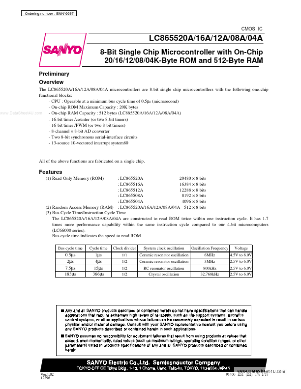
- (1) Read-Only Memory (ROM) : LC865520A 20480 × 8 bits : LC865516A 16384 × 8 bits : LC865512A 12288 × 8 bits : LC865508A 8192 × 8 bits : LC865504A 4096 × 8 bits (2) Random Access Memory (RAM) : LC865520A/16A/12A/08A/04A 512 × 8 bits (3) Bus Cycle Time/Instruction Cycle Time The LC865520A/16A/12A/08A/04A are constructed to read ROM twice within one instruction cycle. It has 1.7 times more performance capability within the same instruction cycle compared to our 4-bit microcomputers (LC66000 series).