K4X56163PI-LG
K4X56163PI-LG is 16Mx16 Mobile DDR SDRAM manufactured by Samsung Semiconductor.
- Part of the K4X56163PI-L comparator family.
- Part of the K4X56163PI-L comparator family.
K4X56163PI
- L(F)E/G 16Mx16 Mobile DDR SDRAM
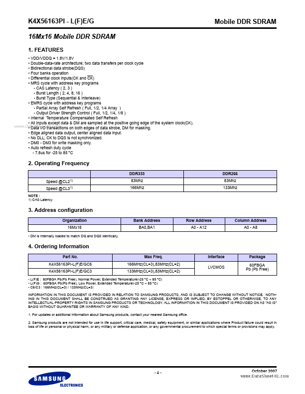
1. Features
- VDD/VDDQ = 1.8V/1.8V
- Double-data-rate architecture; two data transfers per clock cycle
- Bidirectional data strobe(DQS)
- Four banks operation
- Differential clock inputs(CK and CK)
- MRS cycle with address key programs
- CAS Latency ( 2, 3 )
- Burst Length ( 2, 4, 8, 16 )
- Burst Type (Sequential & Interleave)
- EMRS cycle with address key programs
- Partial Array Self Refresh ( Full, 1/2, 1/4 Array )
- Output Driver Strength Control ( Full, 1/2, 1/4, 1/8 )
- Internal Temperature pensated Self Refresh
- All inputs except data & DM are sampled at the positive going edge of the system clock(CK). ..
- Data I/O transactions on both edges of data strobe, DM for masking.
- Edge aligned data output, center aligned data input.
- No DLL; CK to DQS is not synchronized.
- DM0
- DM3 for write masking only.
- Auto refresh duty cycle
- 7.8us for -25 to 85 °C
Mobile DDR SDRAM
2. Operating Frequency
DDR333 Speed @CL2 Speed @CL3
NOTE : 1) CAS Latency
1) 1)
DDR266 83Mhz...