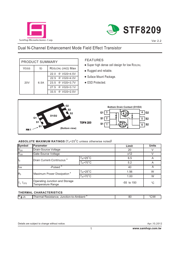
The following content is an automatically extracted verbatim text
from the original manufacturer datasheet and is provided for reference purposes only.
View original datasheet text
Gr Pr
STF8209
Ver 2.2
S a mHop Microelectronics C orp.
Dual N-Channel Enhancement Mode Field Effect Transistor
PRODUCT SUMMARY
V DSS ID R DS(ON) (m Ω) Max
22.0 @ VGS=4.5V 22.5 @ VGS=4.0V 20V 6.5A 23.5 @ VGS=3.7V 27.5 @ VGS=3.1V 33.5 @ VGS=2.5V
FEATURES Super high dense cell design for low R DS(ON). Rugged and reliable. Suface Mount Package. ESD Protected.
G2 S2 G1 S1 S1
P IN 1
Bottom Drain Contact (D1/D2) S2
G1 3 S1 2
T D F N 2X 3
4 G2 5 6 S2 S2
D1/D2
S1
1
(Bottom view)
ABSOLUTE MAXIMUM RATINGS ( T A=25 °C unless otherwise noted ) Symbol VDS VGS ID IDM PD TJ, TSTG Parameter Drain-Source Voltage Gate-Source Voltage Drain Current-Continuous -Pulsed
b a
TA=25°C TA=70°C TA=25°C TA=70°C
Limit 20 ±12 6.5 5.2 40 1.56 1.