SP07N65
Overview
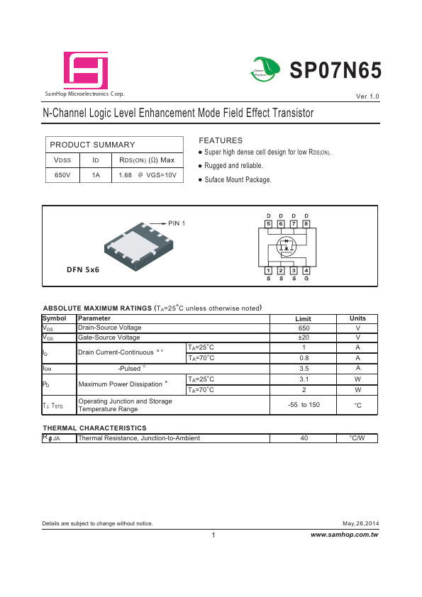
SP07N65Green Product Sa mHop Microelectronics C orp. N-Channel Logic Level Enhancement Mode Field Effect Transistor Ver 1.0 PRODUCT SUMMARY VDSS ID RDS(ON) (Ω) Max 650V 1A 1.68 @ VGS=10V FEATUR...
| Part | SP07N65 |
|---|---|
| Description | N-Channel MOSFET |
| Category | MOSFET |
| Manufacturer | SamHop Microelectronics |
| Size | 96.08 KB |
SP07N65Green Product Sa mHop Microelectronics C orp. N-Channel Logic Level Enhancement Mode Field Effect Transistor Ver 1.0 PRODUCT SUMMARY VDSS ID RDS(ON) (Ω) Max 650V 1A 1.68 @ VGS=10V FEATUR...
| Part Number | Manufacturer | Description |
|---|---|---|
| AP9563GH | Advanced Power Electronics Corp | P-CHANNEL ENHANCEMENT MODE POWER MOSFET |
| FCPF360N65S3R0L | onsemi | N-Channel MOSFET |
| A2SHB | HAOHAI | N-Channel MOSFET |