STP6NA60FP
STP6NA60FP is N - CHANNEL ENHANCEMENT MODE FAST POWER MOS TRANSISTOR manufactured by STMicroelectronics.
DESCRIPTION
This series of POWER MOSFETS represents the most advanced high voltage technology. The optmized cell layout coupled with a new proprietary edge termination concur to give the device low RDS(on) and gate charge, unequalled ruggedness and superior switching performance. APPLICATIONS s HIGH CURRENT, HIGH SPEED SWITCHING s SWITCH MODE POWER SUPPLIES (SMPS) s DC-AC CONVERTERS FOR WELDING EQUIPMENT AND UNINTERRUPTIBLE POWER SUPPLIES AND MOTOR DRIVE
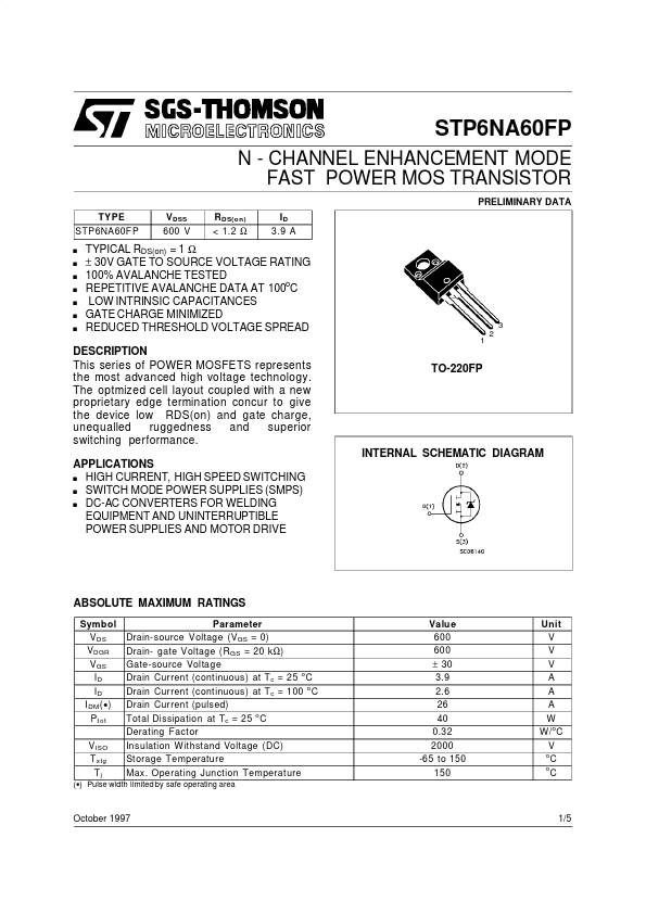
TO-220FP
INTERNAL SCHEMATIC DIAGRAM
ABSOLUTE MAXIMUM RATINGS
Symbol V DS VDGR V GS ID ID I DM (
- ) P t ot V ISO T stg Tj Parameter Drain-source Voltage (V GS = 0) Drain- gate Voltage (R GS = 20 k Ω) Gate-source Voltage Drain Current (continuous) at T c = 25 o C o Drain Current (continuous) at T c = 100 C Drain Current (pulsed) Total Dissipation at Tc = 25 o C Derating Factor Insulation W ithstand Voltage (DC) St orage Temperature Max. Operating Junction Temperature Valu e 600 600 ± 30 3.9 2.6 26 40 0.32 2000 -65 to 150 150 Unit V V V A A A W o W/ C V o C o C
(- ) Pulse width limited by safe operating area
October 1997
1/5
THERMAL DATA
R t hj-ca se R t hj- amb R thc- si nk Tl Thermal Resistance Junction-case Max Thermal Resistance Junction-ambient Max Thermal Resistance Case-sink Typ Maximum Lead Temperature For Soldering Purpose 3.12 62.5 0.5 300 C/W o C/W o C/W o C o
AVALANCHE CHARACTERISTICS
Symb ol I AR E AS Parameter Avalanche Current, Repetitive or Not-Repetitive (pulse width limited by Tj max, δ < 1%) Single Pulse Avalanche Energy (starting Tj = 25 o C, I D = IAR , VDD = 50 V) Max Valu e 6.5 215 Unit A m J
ELECTRICAL CHARACTERISTICS (Tcase = 25 o C unless otherwise specified) OFF
Symb ol V (BR)DSS I DSS I GSS Parameter Drain-source Breakdown Voltage Test Cond ition s I D = 250 µ A V GS = 0 Min. 600 25 250 ± 100 Typ . Max. Un it V µA µA n A
Zero Gate Voltage V DS = Max Rating Drain Current (VGS = 0) V DS = Max Rating Gate-body Leakage V GS = ± 30 V Current (V DS = 0)
T c = 100 o C
ON...