STF6N60M2
Features
Order codes
STF6N60M2 STP6N60M2 STU6N60M2
VDS @ TJmax
RDS(on) max
650 V 1.2 Ω 4.5 A
- Extremely low gate charge
- Lower RDS(on) x area vs previous generation
- Low gate input resistance
- 100% avalanche tested
- Zener-protected
Applications
- Switching applications
AM15572v1
Description
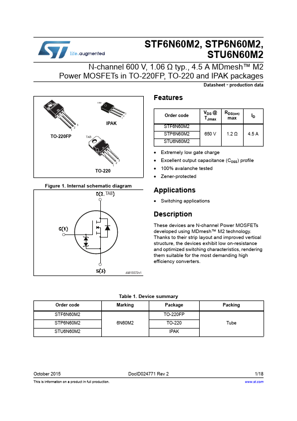
These devices are N-channel Power MOSFETs developed using a new generation of MDmesh™ technology: MDmesh II Plus™ low Qg. These revolutionary Power MOSFETs associate a vertical structure to the pany's strip layout to yield one of the world's lowest on-resistance and gate charge. They are therefore suitable for the most demanding high efficiency converters.
Order codes STF6N60M2 STP6N60M2 STU6N60M2
Table 1. Device summary
Marking
Package
6N60M2
TO-220FP TO-220 IPAK
June 2013
This is information on a product in full production.
Doc ID024771 Rev 1
Packaging Tube
1/18
.st.
Contents
Contents
STF6N60M2, STP6N60M2, STU6N60M2
1 Electrical ratings
- -
- ....