Description
This series of devices implements the second generation of MDmesh™ Technology.
This revolutionary Power MOSFET associates a new vertical structure to the Company’s strip layout to yield one of the world’s lowest on-resistance and gate charge.
Features
- www. DataSheet4U. com Type
VDSS RDS(on) Max (@Tjmax) 710 V 710 V 710 V 710 V 710 V < 0.27 Ω < 0.27 Ω < 0.27 Ω < 0.27 Ω < 0.27 Ω
ID
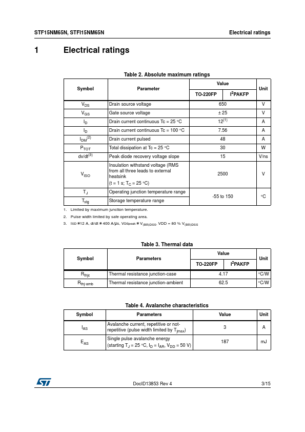
3
STB15NM65N STF15NM65N STI15NM65N STP15NM65N STW15NM65N
15.5 A 15.5 A(1) 15.5 A 15.5 A 15.5 A
1
2
3 12
TO-220
3 1 2
I²PAK
TO-220FP
3 1
2 3
1. Limited only by maximum temperature allowed.
- 100% avalanche tested Low input capacitance and gate charge Low gate input resistance
D²PAK
1
TO-247
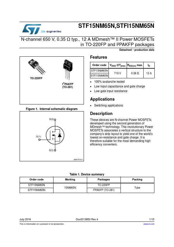
Figure 1.
Internal schematic diagram
Applicatio.
 STF15NM65N Datasheet