Datasheet Details
| Part number | STD2NC50 |
|---|---|
| Manufacturer | STMicroelectronics |
| File Size | 442.61 KB |
| Description | N-CHANNEL MOSFET |
| Datasheet | STD2NC50_STMicroelectronics.pdf |
|
|
|
Overview: N-CHANNEL 500V - 3Ω - 2.2A DPAK/IPAK PowerMesh™II MOSFET TYPE STD2NC50 STD2NC50-1 s s s s s STD2NC50 STD2NC50-1 VDSS 500 V 500 V RDS(on) <4Ω <4Ω ID 2.2 A 2.
| Part number | STD2NC50 |
|---|---|
| Manufacturer | STMicroelectronics |
| File Size | 442.61 KB |
| Description | N-CHANNEL MOSFET |
| Datasheet | STD2NC50_STMicroelectronics.pdf |
|
|
|
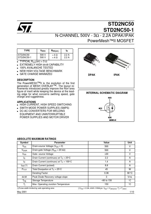
The PowerMESH™II is the evolution of the first generation of MESH OVERLAY™.
The layout refinements introduced greatly improve the Ron*area figure of merit while keeping the device at the leading edge for what concerns swithing speed, gate charge and ruggedness.
APPLICATIONS HIGH CURRENT, HIGH SPEED SWITCHING s SWITH MODE POWER SUPPLIES (SMPS) s DC-AC CONVERTERS FOR WELDING EQUIPMENT AND UNINTERRUPTIBLE POWER SUPPLIES AND MOTOR DRIVER s INTERNAL SCHEMATIC DIAGRAM ABSOLUTE MAXIMUM RATINGS Symbol VDS VDGR VGS ID ID IDM (1) PTOT dv/dt Tstg Tj May 2001 Parameter Drain-source Voltage (VGS = 0) Drain-gate Voltage (RGS = 20 kΩ) Gate- source Voltage Drain Current (continuos) at TC = 25°C Drain Current (continuos) at TC = 100°C Drain Current (pulsed) Total Dissipation at TC = 25°C Derating Factor Peak Diode Recovery voltage slope Storage Temperature Max.
| Part Number | Description |
|---|---|
| STD2NC40-1 | N-CHANNEL MOSFET |
| STD2NC45 | N-CHANNEL MOSFET |
| STD2NC45-1 | N-Channel MOSFET |
| STD2NC60 | N-CHANNEL MOSFET |
| STD2NC70Z | N-CHANNEL MOSFET |
| STD2N50 | N-CHANNEL MOSFET |
| STD2NA50 | N-CHANNEL MOSFET |
| STD2NA60 | N-CHANNEL MOSFET |
| STD2NB25 | N-CHANNEL MOSFET |
| STD2NB40 | N-CHANNEL MOSFET |