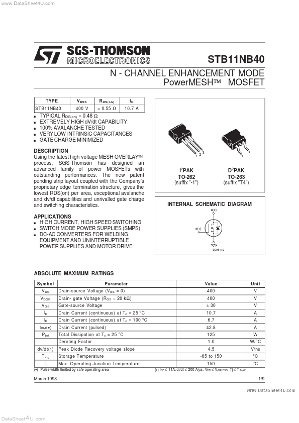
• Part: STB11NB40
  • Description: N - CHANNEL ENHANCEMENT MODE PowerMESH MOSFET
  • Category: MOSFET
  • Manufacturer: STMicroelectronics
  • Size: 247.87 KB
Download STB11NB40 Datasheet PDF
STMicroelectronics
STB11NB40
STB11NB40 is N - CHANNEL ENHANCEMENT MODE PowerMESH MOSFET manufactured by STMicroelectronics.
DESCRIPTION Using the latest high voltage MESH OVERLAY™ process, SGS-Thomson has designed an advanced family of power MOSFETs with outstanding performances. The new patent pending strip layout coupled with the pany’s proprietary edge termination structure, gives the lowest RDS(on) per area, exceptional avalanche and dv/dt capabilities and unrivalled gate charge and switching characteristics. APPLICATIONS s HIGH CURRENT, HIGH SPEED SWITCHING s SWITCH MODE POWER SUPPLIES (SMPS) s DC-AC CONVERTERS FOR WELDING EQUIPMENT AND UNINTERRUPTIBLE POWER SUPPLIES AND MOTOR DRIVE 3 1 I2PAK TO-262 (suffix ”-1”) D2PAK TO-263 (suffix ”T4”) INTERNAL SCHEMATIC DIAGRAM ABSOLUTE MAXIMUM RATINGS Symbol V DS V DGR V GS ID ID IDM ( - ) P t ot dv/dt( 1 ) T stg Tj Parameter Drain-source Voltage (V GS = 0) Drain- gate Voltage (R GS = 20 k Ω ) Gate-source Voltage Drain Current (continuous) at Tc = 25 o C Drain Current (continuous) at Tc = 100 C Drain Current (pulsed) Total Dissipation at Tc = 25 C Derating F actor Peak Diode Recovery voltage slope Storage T emperature Max. O perating Junction Temperature o o Value 400 400 ± 30 10.7 6.7 42.8 125 1.0 4.5 -65 to 150 150 (1) ISD ≤ 11A, di/dt ≤ 200 A/µs, VDD ≤ V(BR)DSS, Tj ≤ TJMAX Uni t V V V A A A W W/ C V/ ns o o o (- ) Pulse width limited by safe operating area March 1998 1/9 Data Sheet 4 U . .. THERMAL DATA R t hj-ca se Rthj -amb R thc- si nk Tl Thermal Resistance Junction-case Max Thermal Resistance Junction-ambient Max Thermal Resistance Case-sink Typ Maximum Lead Temperature For Soldering Purpose 1.0 62.5 0.5 300 C/W o C/W o C/W o C o AVALANCHE CHARACTERISTICS Symb ol I AR E AS Parameter Avalanche Current, Repetitive or Not-Repetitive (pulse width limited by Tj max, δ < 1%) Single Pulse Avalanche Energy (starting Tj = 25 o C, I D = IAR , VDD = 50 V) Max Valu e 10.7 530 Unit A m J ELECTRICAL CHARACTERISTICS (Tcase = 25 o C unless otherwise specified) OFF Symb ol V (BR)DSS I DSS I GSS Parameter Drain-source...