P9NC65FP
P9NC65FP is STP9NC65FP manufactured by STMicroelectronics.
..
N-CHANNEL 650V
- 0.75Ω
- 8A TO-220/TO-220FP Power Mesh™II MOSFET
TYPE STP9NC65 STP9NC65FP s s s s s
STP9NC65 STP9NC65FP
VDSS 650 V 650 V
RDS(on) < 0.90 Ω < 0.90 Ω
ID 8A 8A
TYPICAL RDS(on) = 0.75 Ω EXTREMELY HIGH dv/dt CAPABILITY 100% AVALANCHE TESTED NEW HIGH VOLTAGE BENCHMARK GATE CHARGE MINIMIZED
3 1 2
TO-220
(Available Upon Request)
TO-220FP
DESCRIPTION The Power MESH™II is the evolution of the first generation of MESH OVERLAY™. The layout refinements introduced greatly improve the Ron- area figure of merit while keeping the device at the leading edge for what concerns swithing speed, gate charge and ruggedness. APPLICATIONS HIGH CURRENT, HIGH SPEED SWITCHING s SWITH MODE POWER SUPPLIES (SMPS) s DC-AC CONVERTERS FOR WELDING EQUIPMENT AND UNINTERRUPTIBLE POWER SUPPLIES AND MOTOR DRIVES s
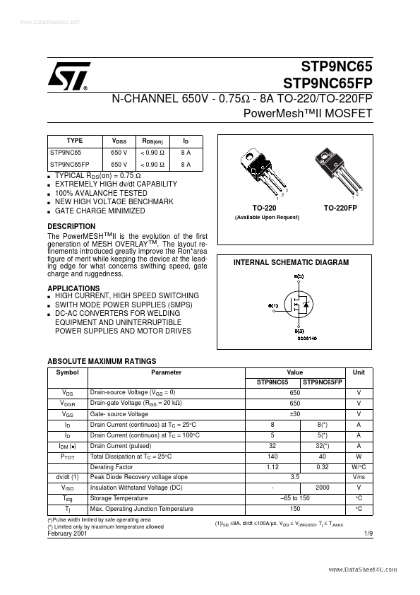
INTERNAL SCHEMATIC DIAGRAM
ABSOLUTE MAXIMUM RATINGS
Symbol VDS VDGR VGS ID ID IDM (q) PTOT dv/dt (1) VISO Tstg Tj Parameter Drain-source Voltage (VGS = 0) Drain-gate Voltage (RGS = 20 kΩ) Gate- source Voltage Drain Current (continuos) at TC = 25°C Drain Current (continuos) at TC = 100°C Drain Current (pulsed) Total Dissipation at TC = 25°C Derating Factor Peak Diode Recovery voltage slope Insulation Withstand Voltage (DC) Storage Temperature Max. Operating Junction Temperature
- 65 to 150 150
(1)ISD ≤8A, di/dt ≤100A/µs, V DD ≤ V(BR)DSS, Tj ≤ TJMAX.
Value STP9NC65 650 650 ±30 8 5 32 140 1.12 3.5 2000 8(- ) 5(- ) 32(- ) 40 0.32 STP9NC65FP
Unit V V V A A A W W/°C V/ns V °C °C
(- )Pulse width limited by safe operating area (- ) Limited only by maximum temperature allowed
February 2001
1/9
..
STP9NC65/FP
THERMAL DATA
TO-220 Rthj-case Rthj-amb Rthc-sink Tl Thermal Resistance Junction-case Max Thermal Resistance Junction-ambient Max Thermal Resistance Case-sink Typ Maximum Lead Temperature For Soldering Purpose 0.89 62.5 0.5 300 TO-220FP 3.12 °C/W °C/W °C/W °C
AVALANCHE CHARACTERISTICS...