L4916 Overview
Description
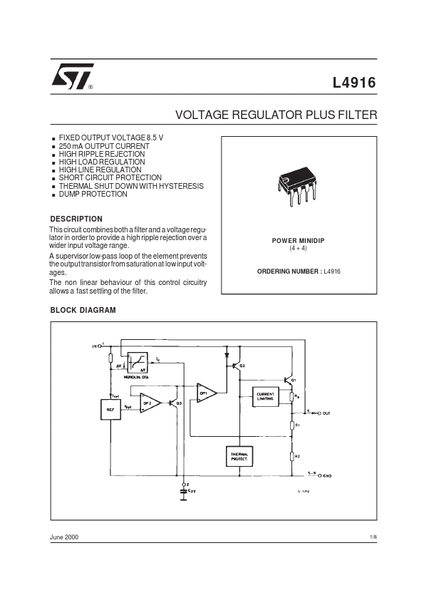
This circuit combinesboth a filter and a voltageregulator in order to provide a high ripple rejection over a wider input voltage range. A supervisor low-pass loop of the element prevents the outputtransistor from saturationat low input voltages.