• Part: HCF40100B
  • Description: 32-STAGE STATIC LEFT/RIGHT SHIFT REGISTER
  • Manufacturer: STMicroelectronics
  • Size: 287.23 KB
Download HCF40100B Datasheet PDF
STMicroelectronics
HCF40100B
HCF40100B is 32-STAGE STATIC LEFT/RIGHT SHIFT REGISTER manufactured by STMicroelectronics.
DESCRIPTION OF ”B” SERIES CMOS DEVICES” data in the 32nd stage is shifted into the first stage when the LEFT/RIGHT CONTROL is low and from the 1st stage to the 32nd stage when the LEFT/RIGHT CONTROL is high. EY (Plastic Package) F (Ceramic Frit Seal Package) DESCRIPTION 
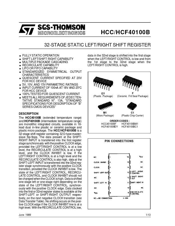
The HCC40100B (extended temperature range) and HCF40100B (intermediate temperature range) are monolithic integrated circuits, available in 16lead dual in-line plastic or ceramic package and plastic micro package. The HCC/HCF40100B is a 32-stage shift register containing 32 D-type masterslave flip-flops. The data present at the SHIFTRIGHT INPUT is transferred into the first register stage synchronously with the positive CLOCK edge, provided the LEFT/RIGHT CONTROL is at a low level, the RECIRCULATE CONTROL is at a high level, and the CLOCK INHIBIT is low. If the LEFT/RIGHT CONTROL is at a high level and the RECIRCULATE CONTROL is also high, data at the SHIFT-LEFT INPUT is transferred into the 32nd register stage synchronously with the positive CLOCK transition, provided the CLOCK INHIBIT is low. The state of the LEFT/RIGHT CONTROL, RECIRCULATE CONTROL, and CLOCK INHIBIT should not be changed when the CLOCK is high. Data is shifted one stage left or one stage right depending on the state of the LEFT/RIGHT CONTROL, synchronously with the positive CLOCK edge. Data clocked into the first or 32nd register states is available at the SHIFT-LEFT or SHIFT-RIGHT OUTPUT respectively, on the next negative CLOCK transition (see Data Transfer Table). No shifting occurs on the positive CLOCK edge if the CLOCK INHIBIT line is at a high level. With the RECIRCULATE CONTROL low, June 1989 M1 (Micro Package) C1 (Plastic Chip Carrier) ORDER CODES : HCC40100BF HCF40100BM1 HCF40100BEY HCF40100BC1 PIN CONNECTIONS 1/13 HCC/HCF40100B FUNCTIONAL DIAGRAM ABSOLUTE MAXIMUM RATINGS Symbol V DD - Vi II Pto t Parameter Supply Voltage : HC C Types H C F Types Input Voltage DC Input Current (any one input) Total Power...