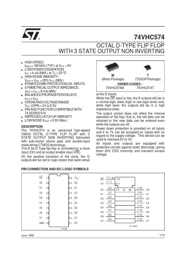
74VHC574
74VHC574 is Octal D-Type Flip-Flop manufactured by STMicroelectronics.
DESCRIPTION
The 74VHC574 is an advanced high-speed CMOS OCTAL D-TYPE FLIP FLOP with 3 STATE OUTPUT NON INVERTING fabricated with sub-micron silicon gate and double-layer metal wiring C2MOS technology. This 8 bit D-Type flip-flop is controlled by a clock input (CK) and an output enable input (OE). On the positive transition of the clock, the Q outputs will be set to logic states that were setup PIN CONNECTION AND IEC LOGIC SYMBOLS
June 1999
1/10
INPUT EQUIVALENT CIRCUIT PIN DESCRIPTION
PIN No 1 2, 3, 4, 5, 6, 7, 8, 9 12, 13, 14, 15, 16, 17, 18, 19 11 10 20 SYMBOL OE D0 to D7 NAME AND FUNCT ION 3 State Output Enable Input (Active LOW) Data Inputs
Q0 to Q7
3 State Outputs
CLOCK GND VCC
Clock Input (LOW to HIGH, edge triggered) Ground (0V) Positive Supply Voltage
TRUTH TABLE
INPUTS OE H L L L
X:Don’t Care Z: High Impedance
OUT PUTS D X X L H Q Z NO CHANGE L H
CK X
LOGIC DIAGRAM
2/10
ABSOLUTE MAXIMUM RATINGS
Symbol VCC VI VO IIK IOK IO Tstg TL Supply Voltage DC Input Voltage DC Output Voltage DC Input Diode Current DC Output Diode Current DC Output Current Storage Temperature Lead Temperature (10 sec) Parameter Value -0.5 to +7.0 -0.5 to +7.0 -0.5 to VCC + 0.5
- 20 ± 20 ± 25 ± 75 -65 to +150 300 Unit V V V m A m A m A m A o o
ICC or IGND DC VCC or Ground Current
Absolute Maximum Ratings are those values beyond which damage to the device may occur. Functional operation under these condition is not implied.
REMENDED OPERATING CONDITIONS
Symbol VCC VI VO Top dt/dv Supply Voltage Input Voltage Output Voltage Operating Temperature Input Rise and Fall Time (see note 1) (VCC = 3.3 ± 0.3V) (V CC = 5.0 ± 0.5V) Parameter Valu e 2.0 to 5.5 0 to 5.5 0 to VCC -40 to +85 0...