HD74LVC1G98 Datasheet Text
..
HD74LVC1G98
Configurable Multiple- Function Gate
REJ03D0013- 0400Z Rev.4.00 Jun. 30, 2004
Description
The HD74LVC1G98 has configurable multiple- function gate in a 6-pin package. The Output state is determined by eight patterns of 3- bit input. The user can choose the logic functions AND, NAND, OR, NOR, INVERTER, Non- Inverted Buffer, Data Selector. Low voltage and high-speed operation is suitable for the battery powered products (e.g., notebook puters), and the low power consumption extends the battery life.
Features
- The basic gate function is lined up as Renesas uni logic series.
- Supply voltage range: 1.65 to 5.5 V Operating temperature range:
- 40 to +85°C
- All inputs VIH (Max.) = 5.5 V (@VCC = 0 V to 5.5 V) All outputs VO (Max.) = 5.5 V (@VCC = 0 V)
- Output current: ±4 mA (@VCC = 1.65 V) ±8 mA (@VCC = 2.3 V) ±24 mA (@VCC = 3.0 V) ±32 mA (@VCC = 4.5 V)
- All the logical input has hysteresis voltage for the slow transition.
- Ordering Information
Part Name HD74LVC1G98CPE HD74LVC1G98CLE Package Type WCSP-6 pin Package Code TBS-6V TBS-6AV Package Abbreviation CP CL Taping Abbreviation (Quantity) E (3,000 pcs/reel)
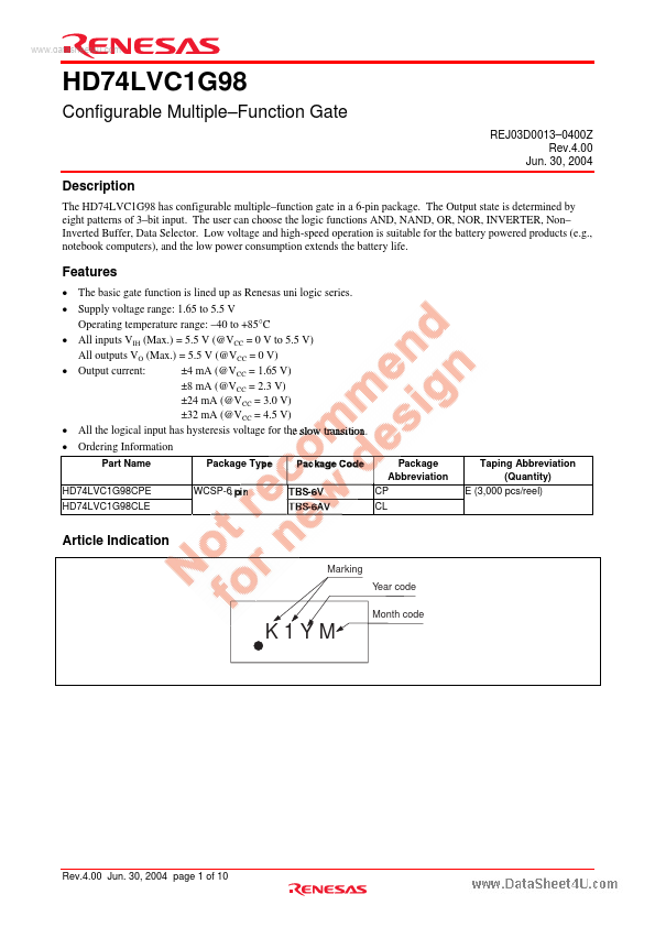
Article Indication
Marking Year code Month code
K1YM
Rev.4.00 Jun. 30, 2004 page 1 of 10
HD74LVC1G98
..
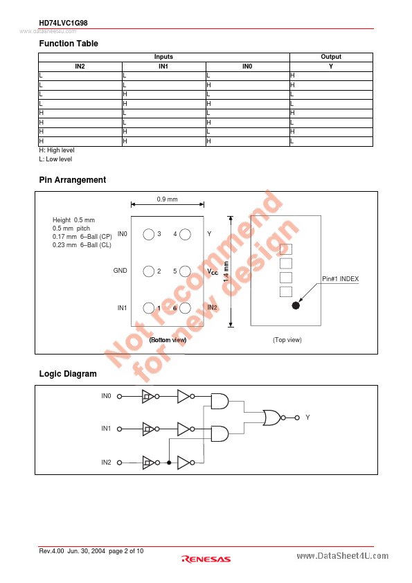
Function Table
IN2 L L L L H H H H H: High level L: Low level L L H H L L H H Inputs IN1 L H L H L H L H IN0 H H L L H L H L Output Y
Pin Arrangement
0.9 mm Height 0.5 mm 0.5 mm pitch 0.17 mm 6- Ball (CP) IN0 0.23 mm 6- Ball (CL)
3
4
Y
GND
2...