V103
V103 is TRIPLE 10-BIT LVDS TRANSMITTER manufactured by Renesas.
Description
The V103 LVDS display interface transmitter is primarily designed to support pixel data transmission between a video processing engine and a digital video display. The data rate supports up to SXGA+ resolutions and can be used in Plasma, Rear Projector, Front Projector, CRT and LCD display applications. It can also be used in other high-bandwidth parallel data applications and provides a low EMI interconnect over a low cost, low bus width cable up to several meters in length.
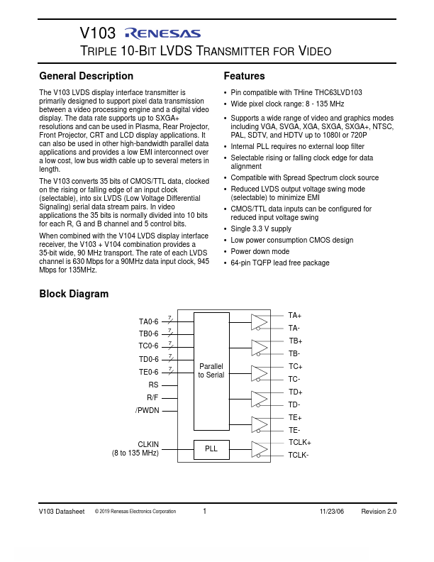
The V103 converts 35 bits of CMOS/TTL data, clocked on the rising or falling edge of an input clock (selectable), into six LVDS (Low Voltage Differential Signaling) serial data stream pairs. In video applications the 35 bits is normally divided into 10 bits for each R, G and B channel and 5 control bits.
When bined with the V104 LVDS display interface receiver, the V103 + V104 bination provides a 35-bit wide, 90 MHz transport. The rate of each LVDS channel is 630 Mbps for a 90MHz data input clock, 945 Mbps for 135MHz.
Features
- Pin patible with THine THC63LVD103
- Wide pixel clock range: 8
- 135 MHz
- Supports a wide range of video and graphics modes including VGA, SVGA, XGA, SXGA, SXGA+, NTSC, PAL, SDTV, and HDTV up to 1080I or 720P
- Internal PLL requires no external loop filter
- Selectable rising or falling clock edge for data alignment
- patible with Spread Spectrum clock source
- Reduced LVDS output voltage swing mode
(selectable) to minimize EMI
- CMOS/TTL data inputs can be configured for reduced input voltage swing
- Single 3.3 V supply
- Low power consumption CMOS design
- Power down mode
- 64-pin TQFP lead free package
Block Diagram
TA0-6 TB0-6 7 TC0-6 7 TD0-6 7 TE0-6 7
R/F
/PWDN
Parallel to Serial
CLKIN (8 to 135 MHz)
TA+ TATB+ TBTC+ TCTD+ TDTE+ TETCLK+ TCLK-
V103 Datasheet
11/23/06
Revision 2.0
TRIPLE 10-BIT LVDS TRANSMITTER FOR VIDEO
Pin Assignment
64 TD4 63 TD3 62 TD2 61 TD1 60 R/F 59 TD0 58 TC6 57 TC5 56 GND 55 TC4 54 TC3 53 TC2 52 TC1...