UPA2592T1H
Overview
- 2.5 V drive available
- Low on-state resistance N-channel RDS(on)1 = 50 mΩ MAX. (VGS = 4.5 V, ID = 2 A) RDS(on)2 = 65 mΩ MAX. (VGS = 2.5 V, ID = 2 A) P-channel RDS(on)1 = 80 mΩ MAX. (VGS = -4.5 V, ID = -2 A) RDS(on)2 = 140 mΩ MAX. (VGS = -2.5 V, ID = -1 A)
- Built-in gate protection diode
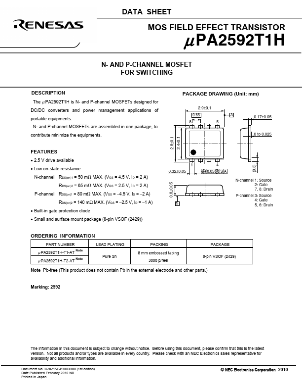
- Small and surface mount package (8-pin VSOF (2429))
- 8±0.05 1 0.32±0.05 S 4 0.05 M S A (0.3) N-channel 1: Source 2: Gate 7, 8: Drain P-channel 3: Source 4: Gate 5, 6: Drain