SLG55321-130010V
Overview
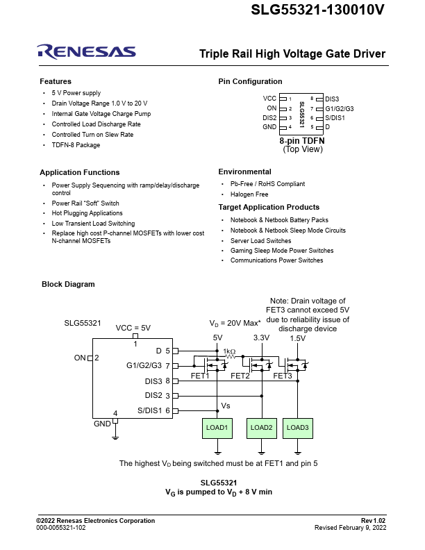
- 5 V Power supply
- Drain Voltage Range 1.0 V to 20 V
- Internal Gate Voltage Charge Pump
- Controlled Load Discharge Rate
- Controlled Turn on Slew Rate
- TDFN-8 Package
| Part | SLG55321-130010V |
|---|---|
| Description | Triple Rail High Voltage Gate Driver |
| Manufacturer | Renesas |
| Size | 255.03 KB |
| Part Number | Manufacturer | Description |
|---|---|---|
| SLG55321-130010V | Silego | High Voltage Gate Driver |