• Part: NP48N055MLE
  • Description: MOS FIELD EFFECT TRANSISTOR
  • Category: Transistor
  • Manufacturer: Renesas
  • Size: 232.75 KB
Download NP48N055MLE Datasheet PDF
Renesas
NP48N055MLE
NP48N055MLE is MOS FIELD EFFECT TRANSISTOR manufactured by Renesas.
- Part of the NP48N055ELE comparator family.
DESCRIPTION These products are N-channel MOS Field Effect Transistors designed for high current switching applications. <R> ORDERING INFORMATION PART NUMBER NP48N055ELE-E1-AY Note1, 2 NP48N055ELE-E2-AY Note1, 2 NP48N055KLE-E1-AY Note1 NP48N055KLE-E2-AY Note1 NP48N055CLE-S12-AZ Note1, 2 NP48N055DLE-S12-AY Note1, 2 NP48N055MLE-S18-AY Note1 NP48N055NLE-S18-AY Note1 LEAD PLATING Pure Sn (Tin) Sn-Ag-Cu Pure Sn (Tin) PACKING Tape 800 p/reel Tube 50 p/tube Notes 1. Pb-free (This product does not contain Pb in the external electrode.) 2. Not for new design PACKAGE TO-263 (MP-25ZJ) typ. 1.4 g TO-263 (MP-25ZK) typ. 1.5 g TO-220 (MP-25) typ. 1.9 g TO-262 (MP-25 Fin Cut) typ. 1.8 g TO-220 (MP-25K) typ. 1.9 g TO-262 (MP-25SK) typ. 1.8 g (TO-220) FEATURES - Channel temperature 175 degree rated - Super low on-state resistance RDS(on)1 = 17 mΩ MAX. (VGS = 10 V, ID = 24 A) RDS(on)2 = 21 mΩ MAX. (VGS = 5 V, ID = 24 A) RDS(on)3 = 24 mΩ MAX. (VGS = 4.5 V, ID = 24 A) - Low input capacitance Ciss = 1970 p F TYP. - 
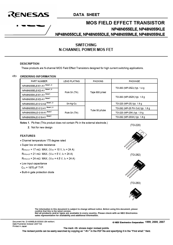
Built-in gate protection diode (TO-262) (TO-263) The information in this document is subject to change without notice. Before using this document, please confirm that this is the latest version. Not all products and/or types are available in every country. Please check with an NEC Electronics sales representative for availability and additional information. Document No. D14095EJ5V0DS00 (5th edition) Date Published October 2007 NS 1999, 2000, 2007 Printed in Japan The mark <R> shows major revised points. The revised points can be easily searched by copying an "<R>" in the PDF file and specifying it in the "Find what:" field. NP48N055ELE, NP48N055KLE, NP48N055CLE, NP48N055DLE, NP48N055MLE, NP48N055NLE ABSOLUTE MAXIMUM RATINGS (TA = 25°C) Drain to Source Voltage (VGS = 0 V) VDSS Gate to Source Voltage (VDS = 0 V) VGSS Drain Current (DC) (TC = 25°C) Drain Current (pulse) Note1 ID(DC) ID(pulse) Total Power Dissipation (TA = 25°C) Total Power Dissipation...