Datasheet Details
| Part number | IDT6V31023 |
|---|---|
| Manufacturer | Renesas |
| File Size | 338.13 KB |
| Description | PCIE GEN1/2/3 CLOCK MULTIPLEXER |
| Datasheet |
 IDT6V31023 Datasheet IDT6V31023 Datasheet
|
|
|
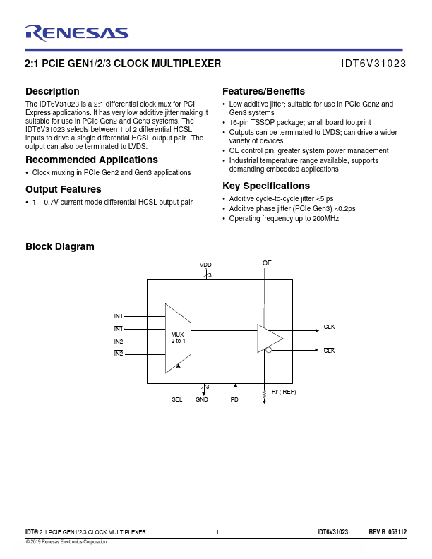
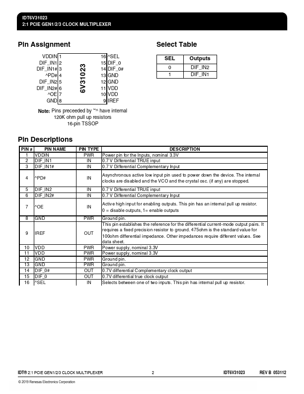
The IDT6V31023 is a 2:1 differential clock mux for PCI Express applications.
It has very low additive jitter making it suitable for use in PCIe Gen2 and Gen3 systems.
The IDT6V31023 selects between 1 of 2 differential HCSL inputs to drive a single differential HCSL output pair.
| Part number | IDT6V31023 |
|---|---|
| Manufacturer | Renesas |
| File Size | 338.13 KB |
| Description | PCIE GEN1/2/3 CLOCK MULTIPLEXER |
| Datasheet |
IDT6V31023 Datasheet
|
|
|
|
| Part Number | Description | Manufacturer |
|---|---|---|
| IDT6V49205A | FREESCALE P10XX AND P20XX SYSTEM CLOCK | Integrated Device Technology |
| IDT6116LA | CMOS Static RAM | Integrated Device Technology |
| IDT6116SA | CMOS Static RAM | Integrated Device Technology |
| IDT61298SA | CMOS STATIC RAM 256K (64K x 4-BIT) | Integrated Device Technology |
| IDT6167LA | CMOS STATIC RAM | Integrated Device Technology |
| Part Number | Description |
|---|---|
| IDT6V31021 | 4-OUTPUT LOW POWER FANOUT BUFFER |
| IDT6V49205A | DDR CLOCK |
| IDT6116LA | CMOS Static RAM |
| IDT6116SA | CMOS Static RAM |
| IDT6167LA | CMOS Static RAM |
The following content is an automatically extracted verbatim text from the original manufacturer datasheet and is provided for reference purposes only.