Datasheet4U Logo Datasheet4U.com

IDT5V41068A PCIE GEN1/2/3 CLOCK MULTIPLEXER

IDT5V41068A Description

2:1 PCIE GEN1/2/3 CLOCK MULTIPLEXER DATASHEET IDT5V41068A .
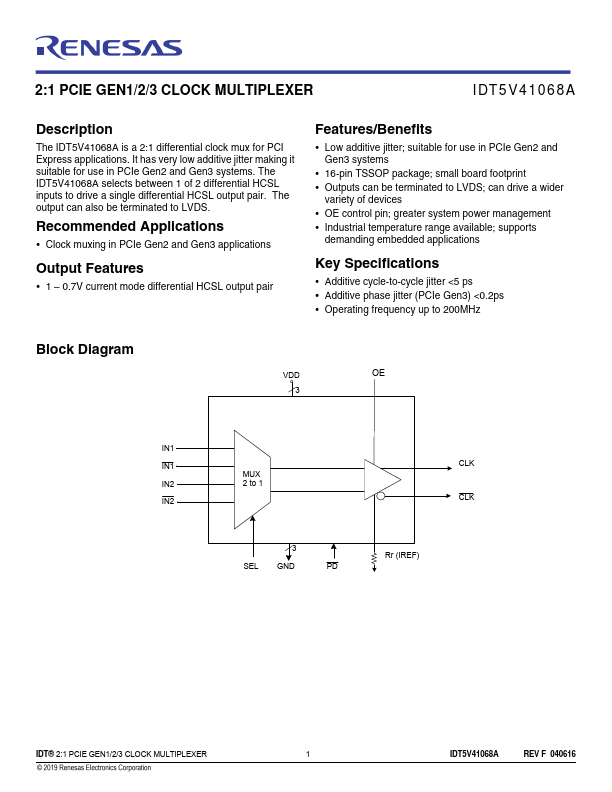
The IDT5V41068A is a 2:1 differential clock mux for PCI Express applications.

IDT5V41068A Features

* 1
* 0.7V current mode differential HCSL output pair Features/Benefits
* Low additive jitter; suitable for use in PCIe Gen2 and Gen3 systems
* 16-pin TSSOP package; small board footprint
* Outputs can be terminated to LVDS; can drive a wider variety of devic

IDT5V41068A Applications

* It has very low additive jitter making it suitable for use in PCIe Gen2 and Gen3 systems. The IDT5V41068A selects between 1 of 2 differential HCSL inputs to drive a single differential HCSL output pair. The output can also be terminated to LVDS. Recommended Applications
* Clock muxing in PC

📥 Download Datasheet

Preview of IDT5V41068A PDF
datasheet Preview Page 2 datasheet Preview Page 3

📁 Related Datasheet

  • IDT5V41065 - 2 OUTPUT PCIE GEN1/2 SYNTHESIZER (IDT)
  • IDT5V41066 - 4 OUTPUT PCIE GEN1/2 SYNTHESIZER (IDT)
  • IDT5V40501 - PLL CLOCK MULTIPLIER (IDT)
  • IDT5V2305 - 2.5V TO 3.3V HIGH PERFORMANCE CLOCK BUFFER (Integrated Device)
  • IDT5V2310 - 2.5V TO 3.3V HIGH PERFORMANCE CLOCK BUFFER (Integrated Device Technology)
  • IDT5V2528 - 2.5V / 3.3V PHASE-LOCK LOOP CLOCK DRIVER ZERO DELAY BUFFER (Integrated Device)
  • IDT5V2528A - 2.5V / 3.3V PHASE-LOCK LOOP CLOCK DRIVER ZERO DELAY BUFFER (Integrated Device)
  • IDT5V5218 - Dual Channel Type-1/Type-2 M-LVDS to LVTTL/LVPECL/LVDS Transceiver (IDT)

📌 All Tags

Renesas IDT5V41068A-like datasheet