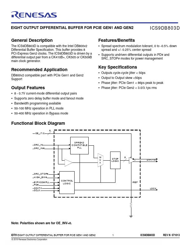
ICS9DB803D Key Features
- 0.7V current-mode differential output pairs
- Supports zero delay buffer mode and fanout mode
- Bandwidth programming available
- 50-100 MHz operation in PLL mode
- 50-400 MHz operation in Bypass mode
- Spread spectrum modulation tolerant, 0 to -0.5% down
- Supports undriven differential outputs in PD# and
- Outputs cycle-cycle jitter < 50ps
- Output to Output skew <50ps
- Phase jitter: PCIe Gen1 < 86ps peak to peak